|
|
|
PDF IDT74FCT841CTSO Data sheet ( Hoja de datos )
| Número de pieza | IDT74FCT841CTSO | |
| Descripción | FAST CMOS BUS INTERFACE LATCHES | |
| Fabricantes | Integrated Device | |
| Logotipo | ||
Hay una vista previa y un enlace de descarga de IDT74FCT841CTSO (archivo pdf) en la parte inferior de esta página. Total 7 Páginas | ||
|
No Preview Available !
Integrated Device Technology, Inc.
FAST CMOS
BUS INTERFACE
LATCHES
IDT54/74FCT841AT/BT/CT/DT
FEATURES:
• Common features:
– Low input and output leakage ≤1µA (max.)
– CMOS power levels
– True TTL input and output compatibility
– VOH = 3.3V (typ.)
– VOL = 0.3V (typ.)
– Meets or exceeds JEDEC standard 18 specifications
– Product available in Radiation Tolerant and Radiation
Enhanced versions
– Military product compliant to MIL-STD-883, Class B
and DESC listed (dual marked)
– Available in DIP, SOIC, SSOP, QSOP, CERPACK
and LCC packages
• Features for FCT841T:
– A, B, C and D speed grades
– High drive outputs (-15mA IOH, 48mA IOL)
– Power off disable outputs permit “live insertion”
DESCRIPTION:
The FCT8xxT series is built using an advanced dual metal
CMOS technology.
The FCT8xxT bus interface latches are designed to elimi-
nate the extra packages required to buffer existing latches
and provide extra data width for wider address/data paths or
buses carrying parity. The FCT841T are buffered, 10-bit wide
versions of the popular FCT373T function. They are ideal for
use as an output port requiring high IOL/IOH.
All of the FCT8xxT high-performance interface family can
drive large capacitive loads, while providing low-capacitance
bus loading at both inputs and outputs. All inputs have clamp
diodes to ground and all outputs are designed for low-capaci-
tance bus loading in high-impedance state.
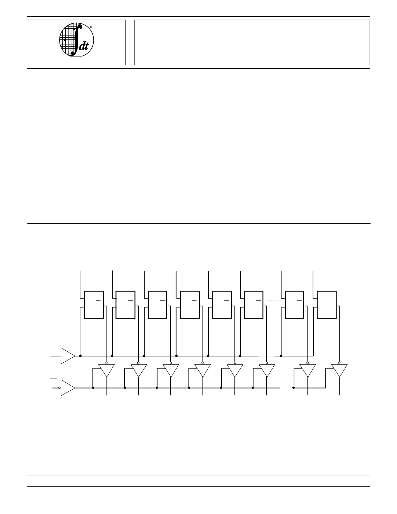
FUNCTIONAL BLOCK DIAGRAM
D0 D1 D2 D3 D4 D5
D8 D9
D
LE Q
D
LE Q
D
LE Q
D
LE Q
D
LE Q
D
LE Q
D
LE Q
D
LE Q
LE
OE
Y0 Y1 Y2 Y3 Y4 Y5
Y8 Y9
2571 drw 01
The IDT logo is a registered trademark of Integrated Device Technology, Inc.
MILITARY AND COMMERCIAL TEMPERATURE RANGES
©1996 Integrated Device Technology, Inc.
6.22
JUNE 1996
2571/6
1
1 page 
IDT54/74FCT841AT/BT/CT/DT
FAST CMOS BUS INTERFACE LATCHES
MILITARY AND COMMERCIAL TEMPERATURE RANGES
SWITCHING CHARACTERISTICS OVER OPERATING RANGE
FCT841AT
FCT841BT
Com'l. Mil. Com'l. Mil.
Symbol
tPLH
tPHL
Parameter
Propagation Delay
DI to YI (LE = HIGH)
tPLH
tPHL
Propagation Delay
LE to YI
tPZH
tPZL
Output Enable Time OE to YI
tPHZ
tPLZ
Output Disable Time OE to Y I
tSU Data to LE Set-up Time
Conditions(1)
CL = 50pF
RL = 500Ω
CL = 300pF(4)
RL = 500Ω
CL = 50pF
RL = 500Ω
CL = 300pF(4)
RL = 500Ω
CL = 50pF
RL = 500Ω
CL = 300pF(4)
RL = 500Ω
CL = 5pF(4)
RL = 500Ω
CL = 50pF
RL = 500Ω
CL = 50pF
Min.(2) Max. Min.(2) Max. Min.(2) Max. Min.(2) Max. Unit
1.5 9.0 1.5 10.0 1.5 6.5 1.5 7.5 ns
1.5 13.0 1.5 15.0 1.5 13.0 1.5 15.0
1.5 12.0 1.5 13.0 1.5 8.0 1.5 10.5 ns
1.5 16.0 1.5 20.0 1.5 15.5 1.5 18.0
1.5 11.5 1.5 13.0 1.5 8.0 1.5 8.5 ns
1.5 23.0 1.5 25.0 1.5 14.0 1.5 15.0
1.5 7.0 1.5 9.0 1.5 6.0 1.5 6.5 ns
1.5 8.0 1.5 10.0 1.5 7.0 1.5 7.5
2.5 — 2.5 — 2.5 — 2.5 — ns
tH Data to LE Hold Time
tW LE Pulse Width HIGH(3)
RL = 500Ω
2.5 — 3.0 — 2.5 — 2.5 — ns
4.0 — 5.0 — 4.0 — 4.0 — ns
NOTES:
1. See test circuit and waveforms.
2. Minimum limits are guaranteed but not tested on Propagation Delays.
3. These parameters are guaranteed but not tested.
4. These conditions are guaranteed but not tested.
2571 tbl 08
SWITCHING CHARACTERISTICS OVER OPERATING RANGE
FCT841CT
FCT841DT
Com'l. Mil. Com'l. Mil.
Symbol
tPLH
tPHL
Parameter
Propagation Delay
DI to YI (LE = HIGH)
tPLH
tPHL
Propagation Delay
LE to YI
tPZH
tPZL
Output Enable Time OE to YI
tPHZ
tPLZ
Output Disable Time OE to Y I
tSU Data to LE Set-up Time
Conditions(1)
CL = 50pF
RL = 500Ω
CL = 300pF(4)
RL = 500Ω
CL = 50pF
RL = 500Ω
CL = 300pF(4)
RL = 500Ω
CL = 50pF
RL = 500Ω
CL = 300pF(4)
RL = 500Ω
CL = 5pF(4)
RL = 500Ω
CL = 50pF
RL = 500Ω
CL = 50pF
Min.(2) Max. Min.(2) Max. Min.(2) Max. Min.(2) Max. Unit
1.5 5.5 1.5 6.3 1.5 4.2 —
— ns
1.5 13.0 1.5 15.0 1.5 8.0 —
—
1.5 6.4 1.5 6.8 1.5 4.0 —
— ns
1.5 15.0 1.5 16.0 1.5 8.0 —
—
1.5 6.5 1.5 7.3 1.5 4.8 —
— ns
1.5 12.0 1.5 13.0 1.5 9.0 —
—
1.5 5.7 1.5 6.0 1.5 4.0 —
— ns
1.5 6.0 1.5 6.3 1.5 4.0 —
—
2.5 — 2.5 — 1.5 — — — ns
tH Data to LE Hold Time
tW LE Pulse Width HIGH(3)
RL = 500Ω
2.5 — 2.5 — 1.0 — — — ns
4.0 — 4.0 — 3.0 — — — ns
NOTES:
1. See test circuit and waveforms.
2. Minimum limits are guaranteed but not tested on Propagation Delays.
3. These parameters are guaranteed but not tested.
4. These conditions are guaranteed but not tested.
2571 tbl 09
6.22 5
5 Page | ||
| Páginas | Total 7 Páginas | |
| PDF Descargar | [ Datasheet IDT74FCT841CTSO.PDF ] | |
Hoja de datos destacado
| Número de pieza | Descripción | Fabricantes |
| IDT74FCT841CTSO | FAST CMOS BUS INTERFACE LATCHES | Integrated Device |
| IDT74FCT841CTSOB | FAST CMOS BUS INTERFACE LATCHES | Integrated Device |
| Número de pieza | Descripción | Fabricantes |
| SLA6805M | High Voltage 3 phase Motor Driver IC. |
Sanken |
| SDC1742 | 12- and 14-Bit Hybrid Synchro / Resolver-to-Digital Converters. |
Analog Devices |
|
DataSheet.es es una pagina web que funciona como un repositorio de manuales o hoja de datos de muchos de los productos más populares, |
| DataSheet.es | 2020 | Privacy Policy | Contacto | Buscar |