|
|
PDF A500K130 Data sheet ( Hoja de datos )
| Número de pieza | A500K130 | |
| Descripción | ProASIC 500K Family | |
| Fabricantes | Actel Corp | |
| Logotipo |  |
|
Hay una vista previa y un enlace de descarga de A500K130 (archivo pdf) en la parte inferior de esta página. Total 70 Páginas | ||
|
No Preview Available !
v3.0
ProASIC™ 500K Family
Features and Benefits
High Capacity
• 100,000 to 475,000 System Gates
• 14k to 63k Bits of Two-Port SRAM
• 106 to 440 User I/Os
Performance
• 33 MHz PCI 32-bit PCI
• Internal System Performance up to 250 MHz
• External System Performance up to 100 MHz
Low Power
• Low Impedance Flash Switches
• Segmented Hierarchical Routing Structure
• Small, Efficient Logic Cells
High Performance Routing Hierarchy
• Ultra Fast Local Network
• Efficient Long Line Network
• High Speed Very Long Line Network
• High Performance Global Network
Nonvolatile and Reprogrammable Flash
Technology
• Live at Power Up
• No Configuration Device Required
• Retains Programmed Design During Power-Down/
Power-Up Cycles
I/O
• Mixed 2.5V/3.3V Support with Individually-Selectable
Voltage and Slew Rate
• 3.3V, PCI Compliance (PCI Revision 2.2)
Secure Programming
The Industry’s Most Effective Security Key Prevents Read
Back of Programming Bit Stream
Standard FPGA and ASIC Design Flow
• Flexibility with Choice of Industry-Standard Front-End
Tools
• Efficient Design Through Front-End Timing and Gate
Optimization
ISP Support
• In-System Programming (ISP) with Silicon Sculptor and
Flash Pro
SRAMs and FIFOs
• Up to 150 MHz Synchronous and Asynchronous Operation
• Netlist Generator Ensures Optimal Usage of Embedded
Memory Blocks
Boundary Scan Test
IEEE Std. 1149.1 (JTAG) Compliant
ProASIC Product Profile
Device
Maximum System Gates
Typical Gates
Maximum Flip-Flops
Embedded RAM Bits
Embedded RAM Blocks (256 X 9)
Logic Tiles
Global Routing Resources
Maximum User I/Os
JTAG
PCI
Package (by Pin Count)
PQFP
PBGA
FBGA
A500K050
100,000
43,000
5,376
14k
6
5,376
4
204
Yes
Yes
208
272
144
A500K130
290,000
105,000
12,800
45k
20
12,800
4
306
Yes
Yes
208
272, 456
144, 256
A500K180
370,000
150,000
18,432
54k
24
18,432
4
362
Yes
Yes
208
456
256
A500K270
475,000
215,000
26,880
63k
28
26,880
4
440
Yes
Yes
208
456
256, 676
February 2002
© 2002 Actel Corporation
1
1 page 
ProASIC™ 500K Family
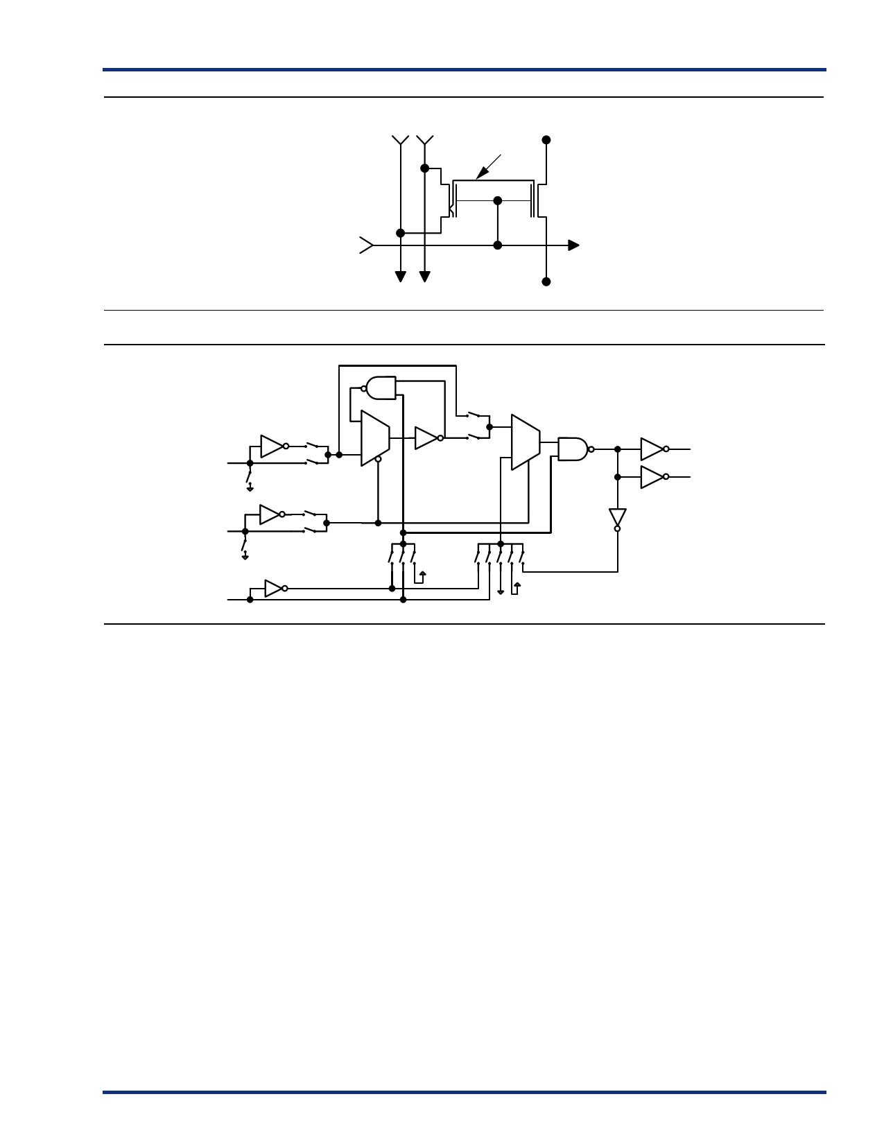
Sel 1 Sel 2
Floating Gate
Switch In
Word
Figure 2 • Flash Switch
Switch Out
In 1
In 2 (CLK)
Local Routing
Efficient Long
Line Routing
In 3 (Reset)
Figure 3 • Core Logic Tile
Routing Resources
The routing structure of the ProASIC 500K devices is
designed to provide high performance through a flexible
four-level hierarchy of routing resources: ultra fast local
resources, efficient long line resources, high speed very long
line resources, and high performance global networks.
The ultra fast local resources are dedicated lines that allow
the output of each tile to connect directly to every input of
the eight surrounding tiles (Figure 4 on page 6).
The efficient long line resources provide routing for longer
distances and higher fanout connections. These resources
vary in length (spanning 1, 2, or 4 tiles), run both vertically
and horizontally, and cover the entire ProASIC device
(Figure 5 on page 6). Each tile can drive signals onto the
efficient long line resources, while the resources can also
access every input of any tile. The routing software
automatically inserts active buffers to limit loading effects
due to distance and fanout.
The high speed very long line resources, spanning across
the entire device with minimal delay, are used to route very
long or very high fanout nets. These resources run vertically
and horizontally, providing multiple access to each group of
tiles throughout the device (Figure 6 on page 7).
The high performance global networks’ clock trees are low
skew, high fanout nets that are accessible from four
dedicated pins or from internal logic (Figure 7 on page 8).
These nets are typically used to distribute clocks, resets,
and other high fanout nets requiring a minimum skew. The
global networks are implemented as clock trees, and signals
can be introduced at any junction. These can be employed
hierarchically, with signals accessing every input on all
tiles.
Clock Resources
ProASIC’s high-drive routing structure provides four global
networks, each accessible from either a dedicated global
pad or a logic tile. Global lines provide optimized worst-case
clock skew of 0.3ns.
v3.0
5
5 Page 
ProASIC™ 500K Family
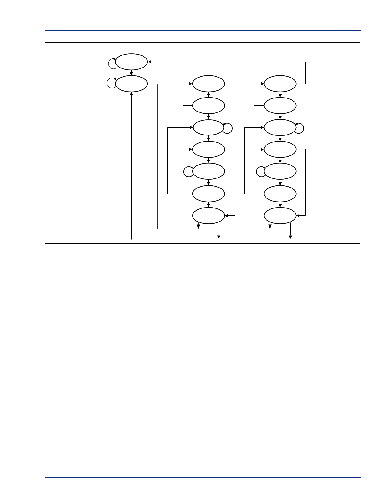
1
Test-Logic
Reset
0
0 Run-Test/
Idle
1
Select-DR-
Scan
0
1
Select-IR-
Scan
0
1
1 Capture-DR
1
0
Shift-DR
0
1
Exit-DR 1
Capture-IR
0
Shift-IR
0
1
Exit-IR 1
00
Pause-DR
1
0 Exit2-DR
1
00
Pause-IR
1
0 Exit2-IR
1
Update-DR
10
Update-IR
10
Figure 11 • TAP Controller State Diagram
User Security
The ProASIC 500K devices have read-protect bits that, once
programmed, lock the entire programmed contents from
being read externally. The user can only reprogram the
device using the security key. This protects it from being
read back and duplicated. Since programmed data is stored
in nonvolatile Flash cells (which act like very small
capacitors), rather than in the wiring, physical
deconstruction cannot be used to compromise data. That
approach would be further hampered by the placement of
the flash cells, beneath the four metal layers (whose
removal could not be accomplished without disturbing the
charge on the floating gate). This is the highest security
provided in the industry. For more information, refer to the
Design Security for Nonvolatile Flash and Antifuse FPGAs
white paper for more information.
Embedded Memory Floorplan
The embedded memory is located across the top of the
device (see Figure 1 on page 4) in 256x9 blocks. Depending
upon the device, 6 to 28 blocks are available to support a
variety of memory configurations. Each block can be
programmed as an independent memory or combined
(using dedicated memory routing resources) to form larger,
more complex memories.
Embedded Memory Configurations
The embedded memory in the ProASIC 500K family provides
great configuration flexibility. While other programmable
vendors typically use single port memories that can only be
transformed into two-port memories by sacrificing half the
memory, each ProASIC block is designed and optimized as a
two-port memory (1 read, 1 write). This provides 63k bits of
total memory for two-port and single port usage in the
A500K270 device.
Each memory can be configured as FIFO or SRAM, with
independent selection of synchronous or asynchronous read
and write ports (Table 3 on page 12). Multiple write ports
are not supported. Additional characteristics include
programmable flags as well as parity check and generation.
Figure 12 and Figure 13 on page 13 show the block diagrams
of the basic SRAM and FIFO blocks. These memories are
designed to operate up to 133 MHz when operated
individually. Each block contains a 256 word deep by 9-bit
wide (1 read, 1 write) memory. The memory blocks may be
combined in parallel to form wider memories or stacked to
form deeper memories (Figure 14 on page 14). This
provides optimal bit widths of 9 (1 block), 18, 36, and 72,
and optimal depths of 256, 512, 768, and 1024. Refer to the
Macro Library Guide for more information.
v3.0
11
11 Page | ||
| Páginas | Total 70 Páginas | |
| PDF Descargar | [ Datasheet A500K130.PDF ] | |
Hoja de datos destacado
| Número de pieza | Descripción | Fabricantes |
| A500K130 | ProASIC 500K Family | Actel Corp |
| Número de pieza | Descripción | Fabricantes |
| SLA6805M | High Voltage 3 phase Motor Driver IC. |
Sanken |
| SDC1742 | 12- and 14-Bit Hybrid Synchro / Resolver-to-Digital Converters. |
Analog Devices |
|
DataSheet.es es una pagina web que funciona como un repositorio de manuales o hoja de datos de muchos de los productos más populares, |
| DataSheet.es | 2020 | Privacy Policy | Contacto | Buscar |
