|
|
|
PDF PC87309 Data sheet ( Hoja de datos )
| Número de pieza | PC87309 | |
| Descripción | PC87309 SuperI/O Plug and Play Compatible Chip in Compact 100-Pin VLJ Packaging | |
| Fabricantes | National Semiconductor | |
| Logotipo | ||
Hay una vista previa y un enlace de descarga de PC87309 (archivo pdf) en la parte inferior de esta página. Total 30 Páginas | ||
|
No Preview Available !
- March 1998
PRELIMINARY
April 1998
PC87309 SuperI/O Plug and Play Compatible Chip
in Compact 100-Pin VLJ Packaging
Highlights
General Description
The PC87309 is a single-chip solution to the most common-
ly used ISA, EISA and MicroChannel® peripherals in a com-
pact, 100-pin VLJ packaging. This fully Plug and Play (PnP)
and PC97 compatible chip conforms to the Plug and Play
ISA Specification Version 1.0a, May 5, 1994, and meets
specifications defined in the PC97 Hardware Design Guide.
The PC87309 incorporates: a Floppy Disk Controller (FDC),
a Mouse and Keyboard Controller (KBC), two enhanced
UARTs, one of which is with Infrared (IR) support, a full
IEEE 1284 parallel port and support for Power Management
(PM). The chip also provides a separate configuration reg-
ister set for each module.
The Infrared (IR) interface complies with the HP-SIR and
SHARP-IR standards, and supports all four basic protocols
for Consumer Remote Control circuitry (RC-5, RC-6, NEC,
RCA and RECS 80).
For flexible UART and IR support, the PC87309 offers two
operation modes:
q Mode 1: Full-IR Mode
UART1 works as UART; UART2 works as fully IR-
compliant device
q Mode 2: Two-UART Mode
Either both UARTs work as UARTs, or UART1 works
as UART and UART2 works as partially IR-compliant
device, providing only IRRX and IRTX support
Outstanding Features
q Full SuperI/O functionality in compact, cost-effective
100-pin VLJ packaging
q PC97 compliant
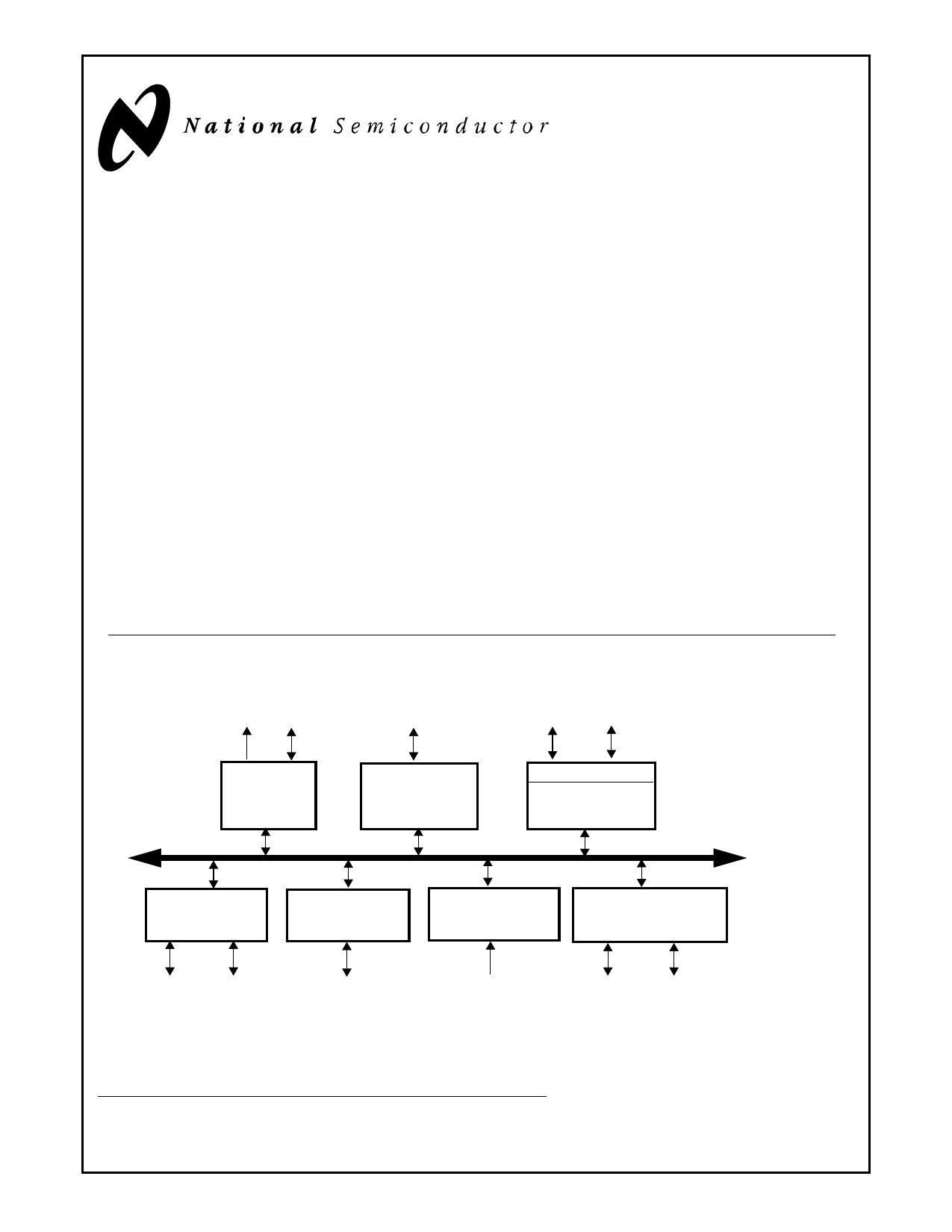
PC87309 Block Diagram
DMA
IRQ Channels
Floppy Drive
Interface
Data Handshake
Plug and Play
(PnP)
Floppy Disk
Controller (FDC)
(Logical Device 0)
High Current Driver
IEEE 1284
Parallel Port
(Logical Device 1)
Serial Port
with IR (UART2)
(Logical Devices 2)
Serial Port
(UART1)
(Logical Devices 3)
Power Management
(PM) Logic
(Logical Device 4)
Mouse and Keyboard
Controller (KBC)
(Logical Devices 5 & 6)
µP Address
Data and
Control
Serial Infrared
Serial
Interface
Control
Data and Ports
Control
TRI-STATE® is a registered trademark of National Semiconductor Corporation.
IBM®, MicroChannel®, PC-AT® and PS/2® are registered trademarks of International Business Machines Corporation.
Microsoft® and Windows® are registered trademarks of Microsoft Corporation.
© 1998 National Semiconductor Corporation
www.national.com
1 page 
Table of Contents
3.3.1
3.3.2
3.3.3
3.3.4
3.3.5
3.3.6
3.3.7
3.3.8
3.3.9
Status Register A (SRA) .............................................................................................. 38
Status Register B (SRB) .............................................................................................. 39
Digital Output Register (DOR) ..................................................................................... 39
Tape Drive Register (TDR) .......................................................................................... 41
Main Status Register (MSR) ........................................................................................ 42
Data Rate Select Register (DSR) ................................................................................ 43
Data Register (FIFO) ................................................................................................... 43
Digital Input Register (DIR) .......................................................................................... 44
Configuration Control Register (CCR) ......................................................................... 45
3.4 THE PHASES OF FDC COMMANDS ....................................................................................... 45
3.4.1 Command Phase ......................................................................................................... 45
3.4.2 Execution Phase .......................................................................................................... 45
3.4.3 Result Phase ............................................................................................................... 47
3.4.4 Idle Phase .................................................................................................................... 47
3.4.5 Drive Polling Phase ..................................................................................................... 48
3.5 THE RESULT PHASE STATUS REGISTERS .......................................................................... 48
3.5.1 Result Phase Status Register 0 (ST0) ......................................................................... 48
3.5.2 Result Phase Status Register 1 (ST1) ......................................................................... 49
3.5.3 Result Phase Status Register 2 (ST2) ......................................................................... 49
3.5.4 Result Phase Status Register 3 (ST3) ......................................................................... 50
3.6 FDC REGISTER BITMAPS ....................................................................................................... 51
3.6.1 Standard ...................................................................................................................... 51
3.6.2 Result Phase Status .................................................................................................... 52
3.7 COMMAND SET ....................................................................................................................... 53
3.7.1 Abbreviations Used in FDC Commands ...................................................................... 54
3.7.2 The CONFIGURE Command ...................................................................................... 55
3.7.3 The DUMPREG Command ......................................................................................... 55
3.7.4 The FORMAT TRACK Command ............................................................................... 56
3.7.5 The INVALID Command .............................................................................................. 58
3.7.6 The LOCK Command .................................................................................................. 60
3.7.7 The MODE Command ................................................................................................. 60
3.7.8 The NSC Command .................................................................................................... 62
3.7.9 The PERPENDICULAR MODE Command ................................................................. 62
3.7.10 The READ DATA Command ....................................................................................... 64
3.7.11 The READ DELETED DATA Command ...................................................................... 66
3.7.12 The READ ID Command ............................................................................................. 67
3.7.13 The READ A TRACK Command ................................................................................. 68
3.7.14 The RECALIBRATE Command ................................................................................... 68
3.7.15 The RELATIVE SEEK Command ................................................................................ 69
3.7.16 The SCAN EQUAL, the SCAN LOW OR EQUAL and the SCAN HIGH OR EQUAL
Commands .................................................................................................................. 69
3.7.17 The SEEK Command .................................................................................................. 70
3.7.18 The SENSE DRIVE STATUS Command .................................................................... 71
3.7.19 The SENSE INTERRUPT Command .......................................................................... 71
3.7.20 The SET TRACK Command ........................................................................................ 72
3.7.21 The SPECIFY Command ............................................................................................ 73
3.7.22 The VERIFY Command ............................................................................................... 74
5 www.national.com
5 Page 
Table of Contents
10.2.15 Group 15 .................................................................................................................... 170
10.2.16 Group 18 .................................................................................................................... 170
10.3 AC ELECTRICAL CHARACTERISTICS .................................................................................. 171
10.3.1 AC Test Conditions .................................................................................................... 171
10.3.2 Clock Timing .............................................................................................................. 171
10.3.3 Microprocessor Interface Timing ............................................................................... 172
10.3.4 Baud Output Timing ................................................................................................... 174
10.3.5 Transmitter Timing ..................................................................................................... 175
10.3.6 Receiver Timing ......................................................................................................... 176
10.3.7 UART, Sharp-IR, SIR and Consumer Remote Control Timing .................................. 178
10.3.8 IRSLn Write Timing ................................................................................................... 179
10.3.9 Modem Control Timing .............................................................................................. 179
10.3.10 FDC DMA Timing ...................................................................................................... 180
10.3.11 ECP DMA Timing ...................................................................................................... 181
10.3.12 UART2 DMA Timing .................................................................................................. 182
10.3.13 Reset Timing ............................................................................................................. 183
10.3.14 FDC - Write Data Timing ........................................................................................... 183
10.3.15 FDC - Drive Control Timing ....................................................................................... 184
10.3.16 FDC - Read Data Timing ........................................................................................... 184
10.3.17 Standard Parallel Port Timing .................................................................................... 185
10.3.18 Enhanced Parallel Port 1.7 Timing ............................................................................ 186
10.3.19 Enhanced Parallel Port 1.9 Timing ............................................................................ 187
10.3.20 Extended Capabilities Port (ECP) Timing .................................................................. 188
Glossary ..................................................................................................................................................... 189
11 www.national.com
11 Page | ||
| Páginas | Total 30 Páginas | |
| PDF Descargar | [ Datasheet PC87309.PDF ] | |
Hoja de datos destacado
| Número de pieza | Descripción | Fabricantes |
| PC87303 | PC87303VUL SuperI/OTM Sidewinder Lite Floppy Disk Controller/ Keyboard Controller/ Real-Time Clock/ Dual UARTs/ IEEE 1284 Parallel Port/ and IDE Inter | National Semiconductor |
| PC87303VUL | PC87303VUL SuperI/OTM Sidewinder Lite Floppy Disk Controller/ Keyboard Controller/ Real-Time Clock/ Dual UARTs/ IEEE 1284 Parallel Port/ and IDE Inter | National Semiconductor |
| PC87306 | PC87306 SuperI/OTM Enhanced Sidewinder Lite Floppy Disk Controller/ Keyboard Controller/ Real-Time Clock/ Dual UARTs/ Infrared Interface/ IEEE 1284 Pa | National Semiconductor |
| PC87306VUL | PC87306 SuperI/OTM Enhanced Sidewinder Lite Floppy Disk Controller/ Keyboard Controller/ Real-Time Clock/ Dual UARTs/ Infrared Interface/ IEEE 1284 Pa | National Semiconductor |
| Número de pieza | Descripción | Fabricantes |
| SLA6805M | High Voltage 3 phase Motor Driver IC. |
Sanken |
| SDC1742 | 12- and 14-Bit Hybrid Synchro / Resolver-to-Digital Converters. |
Analog Devices |
|
DataSheet.es es una pagina web que funciona como un repositorio de manuales o hoja de datos de muchos de los productos más populares, |
| DataSheet.es | 2020 | Privacy Policy | Contacto | Buscar |