|
|
|
PDF RF2173PCBA Data sheet ( Hoja de datos )
| Número de pieza | RF2173PCBA | |
| Descripción | 3V GSM POWER AMPLIFIER | |
| Fabricantes | RF Micro Devices | |
| Logotipo | ||
Hay una vista previa y un enlace de descarga de RF2173PCBA (archivo pdf) en la parte inferior de esta página. Total 14 Páginas | ||
|
No Preview Available !
www.DataSheet4U.com
RF2173
0 3V GSM POWER AMPLIFIER
RoHS Compliant & Pb-Free Product
Typical Applications
• 3V GSM Cellular Handsets
• Commercial and Consumer Systems
• 3V Dual-Band/Triple-Band Handsets
• GPRS Compatible
• Portable Battery-Powered Equipment
Product Description
The RF2173 is a high power, high efficiency power ampli-
fier module offering high performance in GSM or GPRS
applications. The device is manufactured on an advanced
GaAs HBT process, and has been designed for use as
the final RF amplifier in GSM hand-held digital cellular
equipment and other applications in the 800MHz to
950MHz band. On-board power control provides over
70dB of control range with an analog voltage input, and
provides power down with a logic “low” for standby opera-
tion. The device is self-contained with 50Ω input and the
output can be easily matched to obtain optimum power
and efficiency characteristics. The RF2173 can be used
together with the RF2174 for dual-band operation. The
device is packaged in an ultra-small plastic package, min-
imizing the required board space.
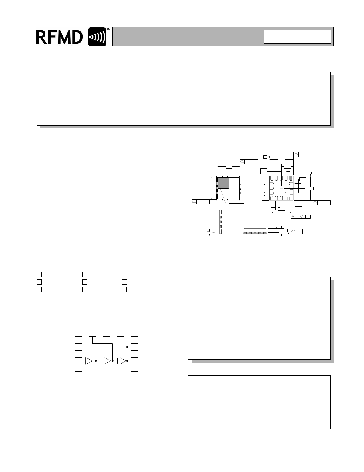
3.75
0.10 C A
2 PLCS
12°
MAX
3.75
0.10 C B
2 PLCS
-B-
0.80
TYP
1.50
SQ.
0.75
0.50
INDEX AREA
Dimensions in mm.
0.45
0.28
Shaded pin is lead 1.
4.00
0.10 C B
2 PLCS
2.00
A
2 1.60
2 PLCS
4.00
3.20
2 PLCS
2.00
0.10 C A
2 PLCS
0.10 M C A B
0.05
0.00
1.00
0.90
0.75
0.65
C
0.05
Optimum Technology Matching® Applied
Si BJT
9GaAs HBT
GaAs MESFET
Si Bi-CMOS
SiGe HBT
Si CMOS
InGaP/HBT
GaN HEMT
SiGe Bi-CMOS
1 16 15 14 13
GND2 2
12 RF OUT
RF IN 3
11 RF OUT
GND1 4
10 RF OUT
56789
Package Style: QFN, 16-Pin, 4x4
Features
• Single 2.7V to 4.8V Supply Voltage
• +36dBm Output Power at 3.5V
• 32dB Gain with Analog Gain Control
• 56% Efficiency
• 800MHz to 950MHz Operation
• Supports GSM and E-GSM
Ordering Information
RF2173
3V GSM Power Amplifier
RF2173PCBA-41X Fully Assembled Evaluation Board
Functional Block Diagram
RF Micro Devices, Inc.
7628 Thorndike Road
Greensboro, NC 27409, USA
Tel (336) 664 1233
Fax (336) 664 0454
http://www.rfmd.com
Rev A7 060921
2-265
1 page 
RF2173
Theory of Operation and Application Information
The RF2173 is a three-stage device with 32 dB gain at
full power. Therefore, the drive required to fully satu-
rate the output is +3dBm. Based upon HBT (Hetero-
junction Bipolar Transistor) technology, the part
requires only a single positive 3V supply to operate to
full specification. Power control is provided through a
single pin interface, with a separate Power Down con-
trol pin. The final stage ground is achieved through the
large pad in the middle of the backside of the package.
First and second stage grounds are brought out
through separate ground pins for isolation from the out-
put. These grounds should be connected directly with
vias to the PCB ground plane, and not connected with
the output ground to form a so called “local ground
plane” on the top layer of the PCB. The output is
brought out through the wide output pad, and forms the
RF output signal path.
The amplifier operates in near Class C bias mode. The
final stage is "deep AB", meaning the quiescent current
is very low. As the RF drive is increased, the final stage
self-biases, causing the bias point to shift up and, at
full power, draws about 2000mA. The optimum load for
the output stage is approximately 1.2Ω. This is the load
at the output collector, and is created by the series
inductance formed by the output bond wires, vias, and
microstrip, and 2 shunt capacitors external to the part.
The optimum load impedance at the RF Output pad is
1.5-j1.7Ω. With this match, a 50Ω terminal impedance
is achieved. The input is internally matched to 50Ω
with just a blocking capacitor needed. This data sheet
defines the configuration for GSM operation.
The input is DC coupled; thus, a blocking cap must be
inserted in series. Also, the first stage bias may be
adjusted by a resistive divider with high value resistors
on this pin to VPC and ground. For nominal operation,
however, no external adjustment is necessary as inter-
nal resistors set the bias point optimally.
VCC1 and VCC2 provide supply voltage to the first and
second stage, as well as provides some frequency
selectivity to tune to the operating band. Essentially,
the bias is fed to this pin through a short microstrip. A
bypass capacitor sets the inductance seen by the part,
so placement of the bypass cap can affect the fre-
quency of the gain peak. This supply should be
bypassed individually with 100pF capacitors before
being combined with VCC for the output stage to pre-
vent feedback and oscillations.
The RF OUT pin provides the output power. Bias for
the final stage is fed to this output line, and the feed
must be capable of supporting the approximately 2A of
current required. Care should be taken to keep the
losses low in the bias feed and output components. A
narrow microstrip line is recommended because DC
losses in a bias choke will degrade efficiency and
power.
While the part is safe under CW operation, maximum
power and reliability will be achieved under pulsed con-
ditions. The data shown in this data sheet is based on
a 12.5% duty cycle and a 600μs pulse, unless speci-
fied otherwise.
The part will operate over a 3.0V to 5.0V range. Under
nominal conditions, the power at 3.5V will be greater
than +34.5dBm at +90°C. As the voltage is increased,
however, the output power will increase. Thus, in a sys-
tem design, the ALC (Automatic Level Control) Loop
will back down the power to the desired level. This
must occur during operation, or the device may be
damaged from too much power dissipation. At 5.0V,
over +38dBm may be produced; however, this level of
power is not recommended, and can cause damage to
the device.
The HBT breakdown voltage is >20V, so there are no
issue with overvoltage. However, under worst-case
conditions, with the RF drive at full power during trans-
mit, and the output VSWR extremely high, a low load
impedance at the collector of the output transistors can
cause currents much higher than normal. Due to the
bipolar nature of the devices, there is no limitation on
the amount of current de device will sink, and the safe
current densities could be exceeded.
High current conditions are potentially dangerous to
any RF device. High currents lead to high channel tem-
peratures and may force early failures. The RF2173
includes temperature compensation circuits in the bias
network to stabilize the RF transistors, thus limiting the
current through the amplifier and protecting the
devices from damage. The same mechanism works to
compensate the currents due to ambient temperature
variations.
To avoid excessively high currents it is important to
control the VAPC when operating at supply voltages
higher than 4.0V, such that the maximum output power
is not exceeded.
Rev A7 060921
2-269
5 Page 
RF2173
PCB Design Requirements
PCB Surface Finish
The PCB surface finish used for RFMD’s qualification process is Electroless Nickel, immersion Gold. Typical thickness is
3μinch to 8μinch Gold over 180μinch Nickel.
PCB Land Pattern Recommendation
PCB land patterns are based on IPC-SM-782 standards when possible. The pad pattern shown has been developed and
tested for optimized assembly at RFMD; however, it may require some modifications to address company specific
assembly processes. The PCB land pattern has been developed to accommodate lead and package tolerances.
PCB Metal Land Pattern
A = 0.51 x 0.89 (mm) Typ.
B = 0.89 x 0.51 (mm) Typ.
C = 1.52 (mm) Sq.
3.20 (mm) Typ.
0.81 (mm)
Typ.
Pin 1
AA AA A
1.73 (mm)
Typ.
0.81 (mm) Typ.
B
B
0.81 (mm) Typ.
B CB
1.60 (mm)
0.94 (mm) Typ.
B
AA
AA
B
A
Figure 1. PCB Metal Land Pattern (Top View)
1.60 (mm)
Typ.
1.73 (mm)
Typ.
Rev A7 060921
2-275
11 Page | ||
| Páginas | Total 14 Páginas | |
| PDF Descargar | [ Datasheet RF2173PCBA.PDF ] | |
Hoja de datos destacado
| Número de pieza | Descripción | Fabricantes |
| RF2173PCBA | 3V GSM POWER AMPLIFIER | RF Micro Devices |
| Número de pieza | Descripción | Fabricantes |
| SLA6805M | High Voltage 3 phase Motor Driver IC. |
Sanken |
| SDC1742 | 12- and 14-Bit Hybrid Synchro / Resolver-to-Digital Converters. |
Analog Devices |
|
DataSheet.es es una pagina web que funciona como un repositorio de manuales o hoja de datos de muchos de los productos más populares, |
| DataSheet.es | 2020 | Privacy Policy | Contacto | Buscar |