|
|
|
PDF RF1K49224 Data sheet ( Hoja de datos )
| Número de pieza | RF1K49224 | |
| Descripción | 3.5A/2.5A/ 30V/ 0.060/0.150 Ohms/ Complementary LittleFET Power MOSFET | |
| Fabricantes | Intersil Corporation | |
| Logotipo | ||
Hay una vista previa y un enlace de descarga de RF1K49224 (archivo pdf) en la parte inferior de esta página. Total 14 Páginas | ||
|
No Preview Available !
Data Sheet
RF1K49224
August 1999 File Number 4330.1
3.5A/2.5A, 30V, 0.060/0.150 Ohms,
Complementary LittleFET™ Power
MOSFET
The RF1K49224 complementary power MOSFET is
manufactured using an advanced MegaFET process. This
process, which uses feature sizes approaching those of LSI
integrated circuits, gives optimum utilization of silicon,
resulting in outstanding performance. It is designed for use
in applications such as switching regulators, switching
converters, motor drivers, relay drivers, and low voltage bus
switches. This device can be operated directly from
intergrated circuits.
Formerly developmental type TA49224.
Ordering Information
PART NUMBER
PACKAGE
BRAND
RF1K49224
MS-012AA
RF1K49224
NOTE: When ordering, use the entire part number. For ordering in
tape and reel, add the suffix 96 to the part number, i.e. RF1K4922496.
Features
• 3.5A, 30V (N-Channel)
2.5A, 30V (P-Channel)
• rDS(ON) = 0.060Ω (N-Channel)
rDS(ON) = 0.150Ω (P-Channel)
• Temperature Compensating PSPICE® Model
• Thermal Impedance PSPICE Model
• Peak Current vs Pulse Width Curve
• UIS Rating Curve
• Related Literature
- TB334 “Guidelines for Soldering Surface Mount
Components to PC Boards”
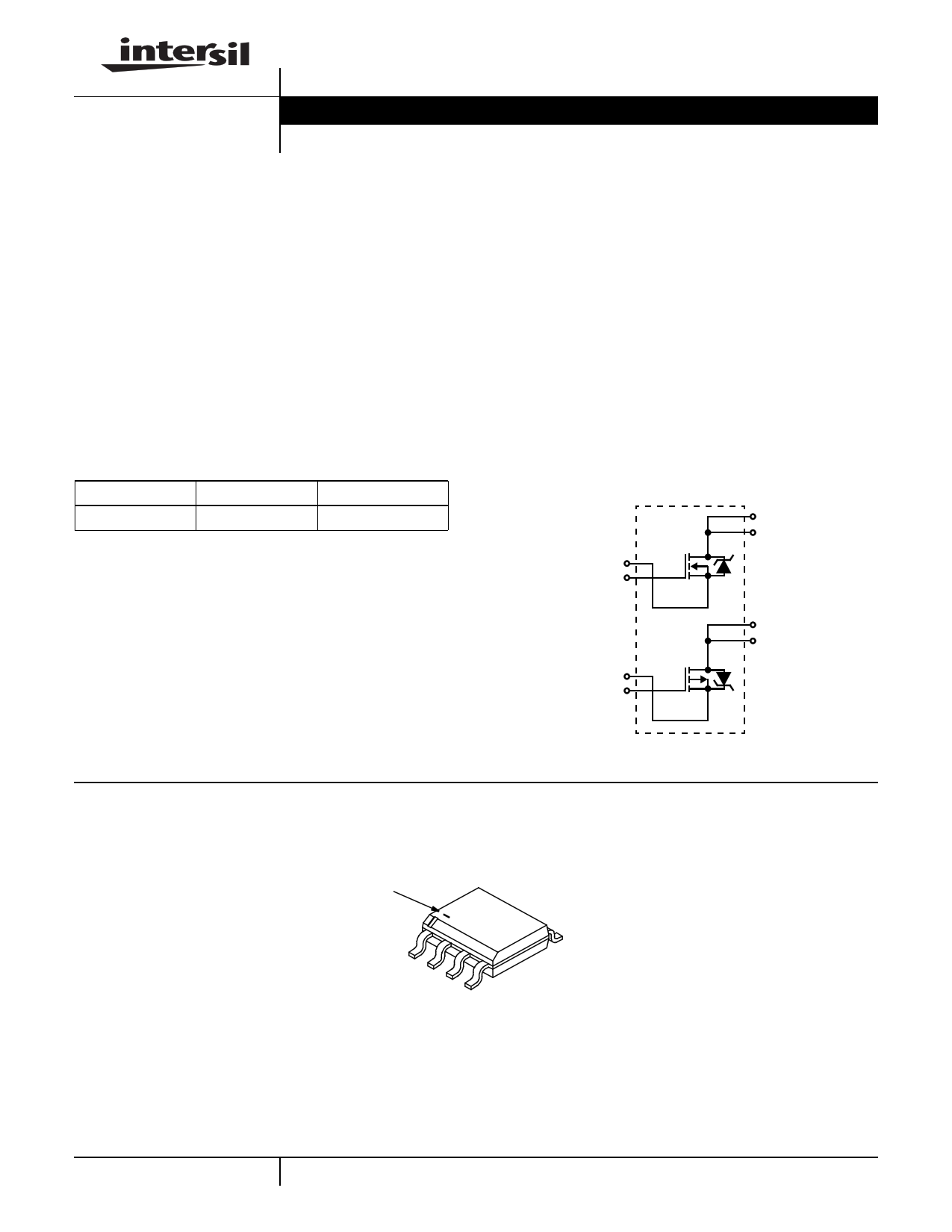
Symbol
S1(1)
G1(2)
D1(8)
D1(7)
S2(3)
G2(4)
D2(6)
D2(5)
Packaging
JEDEC MS-012AA
BRANDING DASH
1
2
3
4
5
9-16
CAUTION: These devices are sensitive to electrostatic discharge; follow proper ESD Handling Procedures.
LittleFET™ is a trademark of Intersil Corporation. PSPICE® is a registered trademark of MicroSim Corporation.
http://www.intersil.com or 407-727-9207 | Copyright © Intersil Corporation 1999
1 page 
RF1K49224
Typical Performance Curves (N-Channel) (Continued)
25
PULSE DURATION = 80µs
DUTY CYCLE = 0.5% MAX
20
25oC
-55oC
15
VDD = 15V
150oC
250 PULSE DURATION = 80µs
DUTY CYCLE = 0.5% MAX
200
ID = 7.0A
ID = 3.5A
VDD = 15V
ID = 1.75A
150
10
5
0
0 1.5 3.0 4.5 6.0
VGS, GATE TO SOURCE VOLTAGE (V)
FIGURE 8. TRANSFER CHARACTERISTICS
7.5
100
ID = 0.5A
50
0
3 4 5 6 7 8 9 10
VGS, GATE TO SOURCE VOLTAGE (V)
FIGURE 9. DRAIN TO SOURCE ON RESISTANCE vs GATE
VOLTAGE AND DRAIN CURRENT
2.0
PULSE DURATION = 80µs
DUTY CYCLE = 0.5% MAX
VGS = 10V, ID = 3.5A
1.5
2.0
VGS = VDS, ID = 250µA
1.5
1.0 1.0
0.5 0.5
0
-80 -40
0 40 80 120 160
TJ, JUNCTION TEMPERATURE (oC)
FIGURE 10. NORMALIZED DRAIN TO SOURCE ON
RESISTANCE vs JUNCTION TEMPERATURE
2.0
ID = 250µA
1.5
1.0
0.5
0
-80 -40 0 40 80 120 160
TJ, JUNCTION TEMPERATURE (oC)
FIGURE 12. NORMALIZED DRAIN TO SOURCE BREAKDOWN
VOLTAGE vs JUNCTION TEMPERATURE
9-20
0
-80 -40
0 40 80 120 160
TJ, JUNCTION TEMPERATURE (oC)
FIGURE 11. NORMALIZED GATE THRESHOLD VOLTAGE vs
JUNCTION TEMPERATURE
100 0
750
500
CISS
COSS
VGS = 0V, f = 1MHz
CISS = CGS + CGD
CRSS = CGD
COSS = CDS + CGD
250
CRSS
0
0 5 10 15 20 25
VDS, DRAIN TO SOURCE VOLTAGE (V)
FIGURE 13. CAPACITANCE vs DRAIN TO SOURCE VOLTAGE
5 Page 
RF1K49224
Soldering Precautions
The soldering process creates a considerable thermal stress
on any semiconductor component. The melting temperature
of solder is higher than the maximum rated temperature of
the device. The amount of time the device is heated to a high
temperature should be minimized to assure device reliability.
Therefore, the following precautions should always be
observed in order to minimize the thermal stress to which
the devices are subjected.
1. Always preheat the device.
2. The delta temperature between the preheat and soldering
should always be less than 100oC. Failure to preheat the
device can result in excessive thermal stress which can
damage the device.
3. The maximum temperature gradient should be less than 5oC
per second when changing from preheating to soldering.
4. The peak temperature in the soldering process should be
at least 30oC higher than the melting point of the solder
chosen.
5. The maximum soldering temperature and time must not
exceed 260oC for 10 seconds on the leads and case of
the device.
6. After soldering is complete, the device should be allowed
to cool naturally for at least three minutes, as forced cool-
ing will increase the temperature gradient and may result
in latent failure due to mechanical stress.
7. During cooling, mechanical stress or shock should be
avoided.
9-26
11 Page | ||
| Páginas | Total 14 Páginas | |
| PDF Descargar | [ Datasheet RF1K49224.PDF ] | |
Hoja de datos destacado
| Número de pieza | Descripción | Fabricantes |
| RF1K49221 | 2.5A/ 60V/ 0.130 Ohm/ ESD Rated/ Dual N-Channel LittleFET Power MOSFET | Intersil Corporation |
| RF1K49223 | 2.5A/ 30V/ 0.150 Ohm/ Dual P-Channel LittleFET Power MOSFET | Fairchild Semiconductor |
| RF1K49223 | 2.5A/ 30V/ 0.150 Ohm/ Dual P-Channel LittleFET Power MOSFET | Intersil Corporation |
| RF1K49224 | 3.5A/2.5A/ 30V/ 0.060/0.150 Ohms/ Complementary LittleFET Power MOSFET | Intersil Corporation |
| Número de pieza | Descripción | Fabricantes |
| SLA6805M | High Voltage 3 phase Motor Driver IC. |
Sanken |
| SDC1742 | 12- and 14-Bit Hybrid Synchro / Resolver-to-Digital Converters. |
Analog Devices |
|
DataSheet.es es una pagina web que funciona como un repositorio de manuales o hoja de datos de muchos de los productos más populares, |
| DataSheet.es | 2020 | Privacy Policy | Contacto | Buscar |