|
|
|
PDF RF2513 Data sheet ( Hoja de datos )
| Número de pieza | RF2513 | |
| Descripción | UHF TRANSMITTER | |
| Fabricantes | RF Micro Devices | |
| Logotipo | ||
Hay una vista previa y un enlace de descarga de RF2513 (archivo pdf) en la parte inferior de esta página. Total 14 Páginas | ||
|
No Preview Available !
11
Typical Applications
• Single- or Dual-Channel LO Source
• FM/FSK Transmitter
• Wireless Data Transmitters
RF2513
UHF TRANSMITTER
• 433/868/915MHz ISM Band Systems
• Wireless Security Systems
Product Description
The RF2513 is a monolithic integrated circuit intended for
use as a low-cost frequency synthesizer and transmitter.
The device is provided in a 24 pin SSOP package and is
designed to provide a phased locked frequency source
for use in local oscillator or transmitter applications. The
chip can be used in FM or FSK applications in the U.S.
915MHz ISM band and European 433MHz or 868MHz
ISM band. The integrated VCO, dual-modulus/dual-divide
(128/129 or 64/65) prescaler, and reference oscillator
require only the addition of an external crystal to provide
a complete phase-locked oscillator. A second reference
oscillator is available to support two channel applications.
0.157
0.150
1
0.344
0.337
0.012
0.008
0.025
0.2440
0.2284
8°MAX
0°MIN
0.0098
0.0040
0.0688
0.0532
0.050 0.0098
0.016 0.0075
Optimum Technology Matching® Applied
üSi BJT
GaAs HBT
GaAs MESFET
Si Bi-CMOS
SiGe HBT
Si CMOS
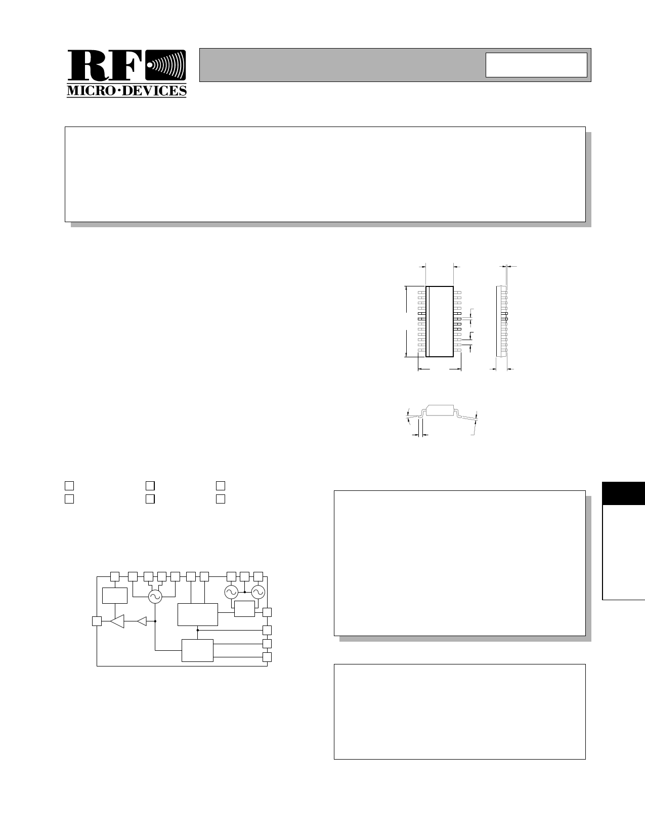
7 16 18 20 22 23 13
Gain
Control
TX OUT 8
Phase
Detector &
Charge Pump
Prescaler
128/129 or
64/65
321
Ref.
Select 24 OSC SEL
12 PRESCL OUT
14 MOD CTRL
15 DIV CTRL
Functional Block Diagram
Package Style: SSOP-24
Features
• Fully Integrated PLL Circuit
• 10mW Output Power at 433MHz
• 2.7V to 5.0V Supply Voltage
• Low Current and Power Down Capability
• 300MHz to 1000MHz Frequency Range
• Narrowband and Wideband FM
Ordering Information
RF2513
UHF Transmitter
RF2513 PCBA-L Fully Assembled Evaluation Board, 433MHz
RF2513 PCBA-M Fully Assembled Evaluation Board, 868MHz
RF2513 PCBA-H Fully Assembled Evaluation Board, 915MHz
RF Micro Devices, Inc.
7625 Thorndike Road
Greensboro, NC 27409, USA
Tel (336) 664 1233
Fax (336) 664 0454
http://www.rfmd.com
11
Rev B8 010509
11-23
1 page 
RF2513
RF2513 Theory of Operation
Introduction
The RF2513 is a low-cost FM/FSK UHF transmitter
designed for applications operating within the 300MHz
to 1000MHz frequency range. It is particularly intended
for 315/433/868MHz band systems, remote keyless
entry systems, and FCC Part 15.231 periodic transmit-
ters. It can also be used as a single- or dual-channel
local oscillator signal source. The integrated VCO,
phase detector, prescaler, and reference oscillator
require only the addition of an external crystal to pro-
vide a complete phase-locked loop.
The RF2513 is provided in a 24-pin SSOP-24 package
and is designed to operate from a supply voltage rang-
ing from 2.2V to 5.0V, accommodating designs using
three NiCd battery cells, two AAA flashlight cells, or a
lithium button battery. The device is capable of provid-
ing up to 10mW output power into a 50Ω load
(+10dBm) and is intended to comply with FCC require-
ments for unlicensed remote control transmitters.
RF2513 Functional Blocks
A PLL consists of a reference oscillator, phase detec-
tor, loop filter, voltage controlled oscillator (VCO), and
a programmable divider in the feedback path. The
RF2513 includes all of these internally, except for the
loop filter and the reference oscillator’s crystal and two
feedback capacitors.
The reference oscillators are Colpitts type oscillators.
Pins 1 (OSC B2), 2 (OSC E), and 3 (OSC B1) provide
connections to the internal transistors used as refer-
ence oscillators. The Colpitts configuration is a low
parts-count topology with reliable performance and
reasonable phase noise. Alternatively, an external sig-
nal could be injected into the base of either transistor.
In either case, the drive level should be around
500mVPP. This level prevents overdriving the device
and keeps phase noise and reference spurs minimal.
The user sets which oscillator is operational by setting
pin 24 (OSC SEL) either high or low. This allows the
implementation of two channel systems.
The prescaler divides the Voltage Controlled Oscilla-
tor (VCO) frequency down by either 64/65 or 128/129,
using a series of flip-flops, depending upon the logic
level present at pin 15 (DIV CTRL). A high logic level
will select the 64/65 divisor. A low logic level will select
the 128/129 divisor. This divided signal is then fed into
the phase detector where it is compared with the refer-
ence frequency.
Rev B8 010509
In addition to the DIV CTRL setting, one also sets the
prescaler modulus by setting pin 14 (MOD CTRL)
either high or low. A high logic level will select the 64/
128 divisor. A low logic level will select the 65/129 divi-
sor.
Pin 12 (PRESCL OUT) provides access to the pres-
caler output. This is used for interfacing to an external
PLL IC.
The RF2513 contains an onboard phase detector and
charge pump. The phase detector compares the
phase of the reference oscillator to the phase of the
VCO. The phase detector is implemented using flip-
flops in a topology referred to as either “digital phase/
frequency detector” or “digital tri-state comparator”.
The circuit consists of two D flip-flops whose outputs
are combined with a NAND gate which is then tied to
the reset on each flip-flop. The outputs of the flip-flops
are also connected to the charge pump. Each flip-flop
output signal is a series of pulses whose frequency is
related to the flip-flop input frequency.
When both inputs of the flip-flops are identical, the sig-
nals are both frequency and phase locked. If they are
different, they will provide signals to the charge pump
which will either charge or discharge the loop filter or
enter into a high impedance state. This is where the
name “tri-state comparator” comes from.
The main benefit of this type of detector it’s ability to
correct for errors in both phase and frequency. When
locked, the detector uses phase error for correction.
When unlocked, it will use the frequency error for cor-
rection. This type of detector will lock under all condi-
tions.
The prescaler and the phase detector bias voltage is
brought out through pin 13 (VREF P). This allows
bypassing of the of these two circuits to filter the refer-
ence crystal frequency.
The charge pump consists of two transistors, one for
charging the loop filter and the other for discharging
the loop filter. It’s inputs are the outputs of the phase
detector flip-flops. Since there are two flip-flops, there
are four possible states. If both amplifier inputs are low,
then the amplifier pair goes into a high impedance
state, maintaining the charge on the loop filter. The
state where both inputs are high will not occur. The
other states are either charging or discharging the loop
filter. The loop filter integrates the pulses coming from
11
11-27
5 Page 
RF2513
Evaluation Board Schematic
L (433MHz) Board
AUDIO
P1-1
P1-3
P1
1 LVL ADJ
2 GND
3 PLL ON
R5*
0Ω
R3*
0Ω
R4*
0Ω
C21
3-10 pF
D2* D1*
PLL ON
VCC
LVL ADJ
J1
RF OUT
C18
100 nF
50 Ω µstrip
C19
8 pF
X2*
C4
10 nF
L1
22 nH
C6
15 pF
C3
100 pF
C2*
100 pF
C5
100 pF
L2
22 nH
C7
8 pF
X1
6.78 MHz
C1
100 pF
C8
100 pF
1
2
Ref
Select
3
4
Phase
5 Detector/
Charge Pump
6
Gain
7 Control
8
9
VCC
C9
10 nF
C10
100 pF
10
Prescaler
11
24
23
22
21
20
19
18
17
16
15
14
P2-1
P2-3
P2
1 PRESC OUT
2 GND
3 TX EN
P3-1
P3-3
P3-5
P3
1 AUDIO
2 GND
P4-1
3 OSCSLT P4-3
4 GND
5 VCC
P4
1 DIV 64
2 GND
3 MOD CTL
OSC SEL
C17
2.2 nF
C16
22 nF
L3
39 nH
R1
4.7 kΩ
L4
39 nH
L5
220 nH
C12
10 nF
C13
100 pF
C14
4.7 µF
50 Ω µstrip
J2
MOD IN
DIV 64
MOD CTL
TX EN
PRESC OUT
R2*
12 13
C11
0.1 µF
2513400A
11
Rev B8 010509
11-33
11 Page | ||
| Páginas | Total 14 Páginas | |
| PDF Descargar | [ Datasheet RF2513.PDF ] | |
Hoja de datos destacado
| Número de pieza | Descripción | Fabricantes |
| RF2510 | VHF/UHF TRANSMITTER | RF Micro Devices |
| RF2512 | UHF TRANSMITTER | RF Micro Devices |
| RF2513 | UHF TRANSMITTER | RF Micro Devices |
| RF2514 | VHF/UHF TRANSMITTER | RF Micro Devices |
| Número de pieza | Descripción | Fabricantes |
| SLA6805M | High Voltage 3 phase Motor Driver IC. |
Sanken |
| SDC1742 | 12- and 14-Bit Hybrid Synchro / Resolver-to-Digital Converters. |
Analog Devices |
|
DataSheet.es es una pagina web que funciona como un repositorio de manuales o hoja de datos de muchos de los productos más populares, |
| DataSheet.es | 2020 | Privacy Policy | Contacto | Buscar |