|
|
PDF UPD72001C-A8 Data sheet ( Hoja de datos )
| Número de pieza | UPD72001C-A8 | |
| Descripción | MULTI-PROTOCOL SERIAL CONTROLLERS | |
| Fabricantes | NEC | |
| Logotipo |  |
|
Hay una vista previa y un enlace de descarga de UPD72001C-A8 (archivo pdf) en la parte inferior de esta página. Total 30 Páginas | ||
|
No Preview Available !
DATA SHEET
MOS INTEGRATED CIRCUIT
µPD72001-11, 72001-A8
MULTI-PROTOCOL SERIAL CONTROLLERS
DESCRIPTION
The µPD72001-11 is an MPSC (Multi-Protocol Serial Controller) which is a general-purpose communication LSI
equipped with two sets of bidirectional parallel/serial converter circuits for data communication. This controller has
a transmitter function to convert the parallel data output by a data terminal into serial data and transmit this data to
a data transmission system such as a modem, and a receiver function to convert the serial data output by the data
transmission system into parallel data.
The MPSC can be used with data communications equipment with a variety of communication modes such as the
generally and widely used start-stop synchronization mode, and the HDLC mode which is used for high-speed
communication.
The µPD72001-A8 is a low-voltage model.
For this product, the following documents are separately available. Read these documents as well as this Data
Sheet.
• User’s Manual (S12472E)
(I) (S12753E)
• Application Notes (II) (On preparation)
(III) (On preparation)
FEATURES
• Two sets of parallel/serial circuits supporting three modes: start-stop synchronization, character synchronization,
and bit synchronization modes
→ Easy application to a system supporting two or more communication protocols such as a protocol converter or
ISDN terminal adapter
• DPLL (Digital Phase Locked Loop), baud rate generator, and crystal oscillation circuit for transmission/reception
clock
→ Helps reduce cost by decreasing the number of external circuits
• Many variations with power-saving features and small package size
→ Easy application to portable terminals and high-accuracy portable terminals
The features common to the µPD72001-11 and 72001-A8 are explained as the features of the MPSC in this
document.
The information in this document is subject to change without notice.
Document No. S12184EJ7V0DS00 (7th edition)
Date Published November 1997 N
Printed in Japan
The mark shows major revised points.
©
1997
1 page 
µPD72001-11, 72001-A8
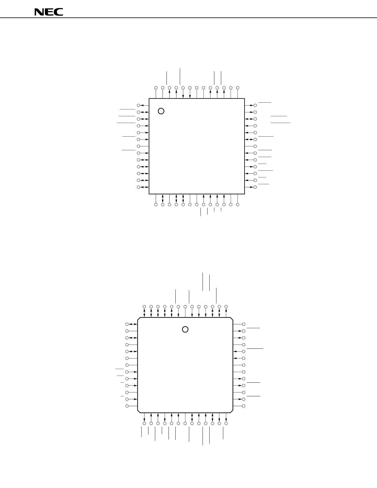
• 52-pin plastic QFP (14 × 14 mm) : µPD72001GC-11-3B6, µPD72001GC-A8-3B6
TXDA
TRXCA
XI2A/SYNCA
XI1A/STRXCA
RXCA
CTSA
IC
DCDA
D7
D6
D5
D4
D3
52 51 50 49 48 47 46 45 44 43 42 41 40
1 39
2 38
3 37
4 36
5 35
6 34
7 33
8 32
9 31
10 30
11 29
12 28
13 27
14 15 16 17 18 19 20 21 22 23 24 25 26
RTSB
TXDB
XI2B/SYNCB
XI1B/STRXCB
RXDB
TRXCB
IC
DCDB
CTSB
INT
INTAK
PRI
PRO
NC: No Connection
IC : Internally Connected (Leave this pin unconnected.)
• 52-pin plastic QFJ (750 × 750 mil) : µPD72001L-11
D2
NC
D1
NC
D0
GND
GND
WR
RD
C/D
NC
B/A
NC
7 6 5 4 3 2 1 52 51 50 49 48 47
8 46
9 45
10 44
11 43
12 42
13 41
14 40
15 39
16 38
17 37
18 36
19 35
20 34
21 22 23 24 25 26 27 28 29 30 31 32 33
NC
RTSA
DRQRXA
NC
RESET
CLK
VDD
VDD
DRQTXA
DTRA/DRQTXB
NC
DTRB/DRQRXB
NC
5
5 Page 
µPD72001-11, 72001-A8
(a) When CR2A: D1, D0 = “0, 0” or “0, 1”
This pin functions as the DTRB output pin. The function of this pin is the same as the DTRA pin, except this
pin is used with channel B.
(b) When CR2A: D1, D0 = “1, 0”
This pin functions as the DRQRXB output pin. The function of this pin is the same as the DRQRxA pin, except
this pin is used with channel B.
(18) CTSA (Clear to Send A) and CTSB (Clear to Send B) ... Input
This pin is a general-purpose input pin and can be used to control a modem, etc. Changes in the status of this
pin affect the latching operation of the E/S bit. When E/S INT is enabled (CR1: D0 = “1”), the E/S interrupt is
generated.
If the Auto Enable mode (CR3: D5 = “1”) is set, the transmitter can be controlled by using the TX Enable bit (CR5:
D3) and this pin. This is illustrated in Table 1-3.
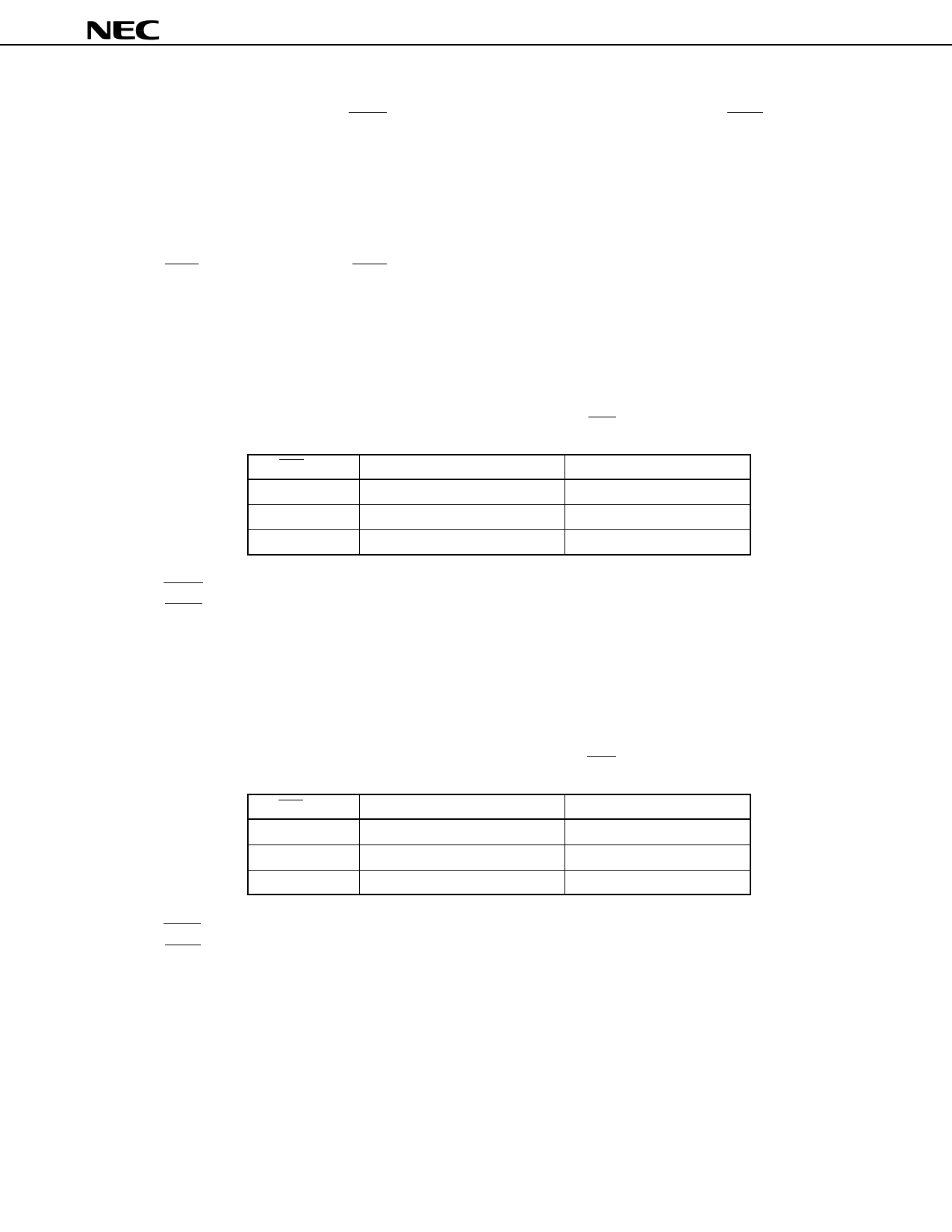
Table 1-3. Auto Enable Mode and CTS Pin
CTS Pin
L
H
H or L
TX Enable Bit
1
1
0
Transmitter Status
Enabled
Disabled
Disabled
(19) DCDA (Data Carrier Detect A) ... Input
DCDB (Data Carrier Detect B) ... Input
These are general-purpose input pins and can be used to control a modem, etc. Changes in the status of this
pin affect the latching operation of the E/S bit. When E/S INT is enabled (CR1: D0 = “1”), the E/S interrupt is
generated.
If the Auto Enable mode (CR3: D5 = “1”) is set, the receiver can be controlled by using the RX Enable bit (CR3:
D0) and this pin. This is illustrated in Table 1-4.
Table 1-4. Auto Enable Mode and DCD Pin
DCD Pin
L
H
H or L
RX Enable Bit
1
1
0
Receiver Status
Enabled
Disabled
Disabled
(20) RTSA (Request to Send A) ... Output
RTSB (Request to Send B) ... Output
These are general-purpose output pins and can be used to control a modem, etc. The operations of these pins
differ depending on the setting of the operation protocol and the setting of the Auto Enable bit, as shown in Table
1-5.
11
11 Page | ||
| Páginas | Total 30 Páginas | |
| PDF Descargar | [ Datasheet UPD72001C-A8.PDF ] | |
Hoja de datos destacado
| Número de pieza | Descripción | Fabricantes |
| UPD72001C-A8 | MULTI-PROTOCOL SERIAL CONTROLLERS | NEC |
| Número de pieza | Descripción | Fabricantes |
| SLA6805M | High Voltage 3 phase Motor Driver IC. |
Sanken |
| SDC1742 | 12- and 14-Bit Hybrid Synchro / Resolver-to-Digital Converters. |
Analog Devices |
|
DataSheet.es es una pagina web que funciona como un repositorio de manuales o hoja de datos de muchos de los productos más populares, |
| DataSheet.es | 2020 | Privacy Policy | Contacto | Buscar |
