|
|
PDF V54C3256164VBUC Data sheet ( Hoja de datos )
| Número de pieza | V54C3256164VBUC | |
| Descripción | LOW POWER 256Mbit SDRAM 3.3 VOLT/ 54-BALL SOC BGA 54-PIN TSOPII 16M X 16 | |
| Fabricantes | Mosel Vitelic Corp | |
| Logotipo |  |
|
Hay una vista previa y un enlace de descarga de V54C3256164VBUC (archivo pdf) en la parte inferior de esta página. Total 30 Páginas | ||
|
No Preview Available !
MOSEL VITELIC
V54C3256164VBUC/T
LOW POWER 256Mbit SDRAM
3.3 VOLT, 54-BALL SOC BGA
54-PIN TSOPII 16M X 16
PRELIMINARY
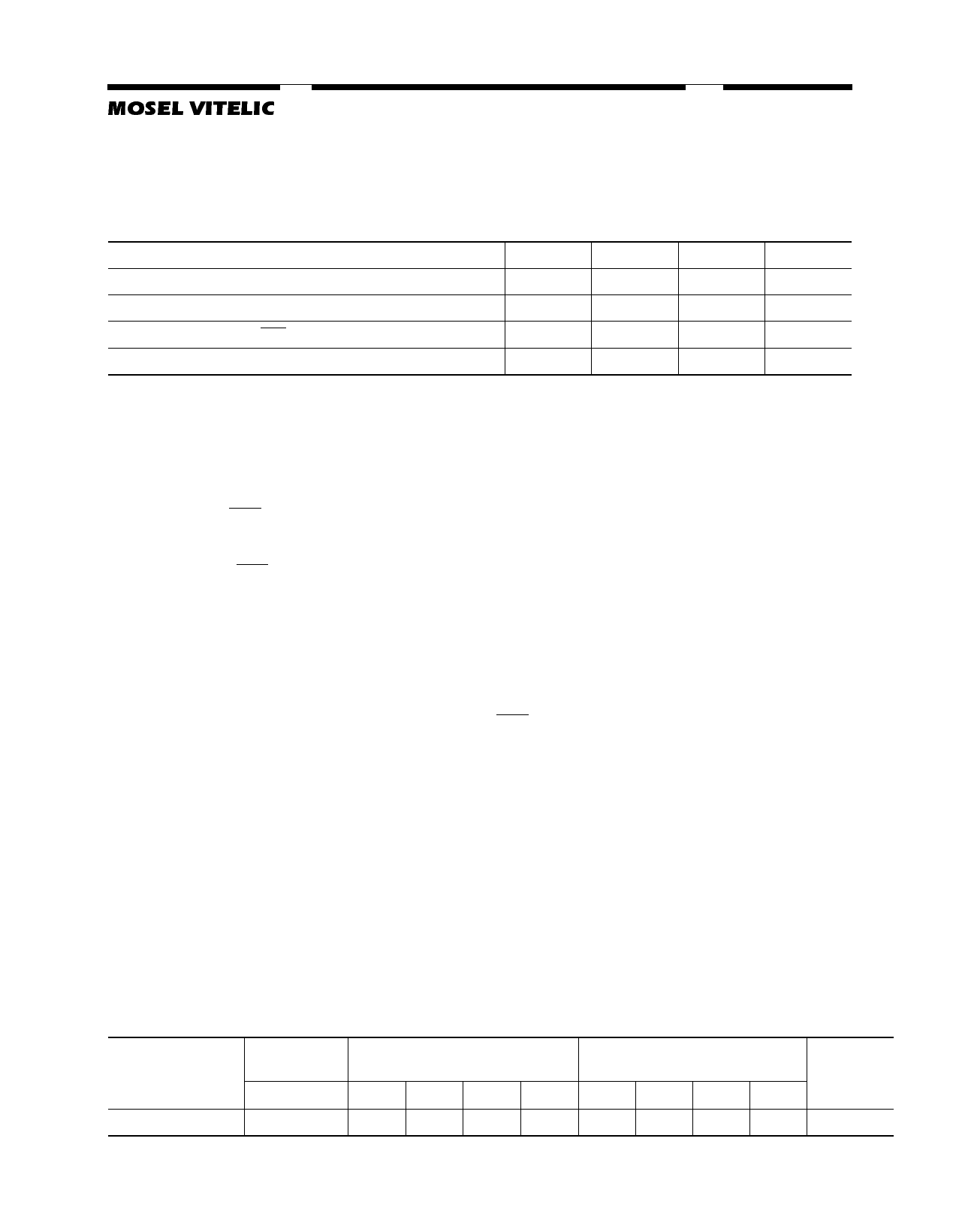
System Frequency (fCK)
Clock Cycle Time (tCK3)
Clock Access Time (tAC3) CAS Latency = 3
Clock Access Time (tAC2) CAS Latency = 2
6
166 MHz
6 ns
5.4 ns
5.4 ns
7PC
143 MHz
7 ns
5.4 ns
5.4 ns
7
143 MHz
7 ns
5.4 ns
6 ns
8PC
125 MHz
8 ns
6 ns
6 ns
Features
■ 4 banks x 4Mbit x 16 organization
■ High speed data transfer rates up to 166 MHz
■ Full Synchronous Dynamic RAM, with all signals
referenced to clock rising edge
■ Single Pulsed RAS Interface
■ Data Mask for Read/Write Control
■ Four Banks controlled by BA0 & BA1
■ Programmable CAS Latency: 2, 3
■ Programmable Wrap Sequence: Sequential or
Interleave
■ Programmable Burst Length:
1, 2, 4, 8 for Sequential Type
1, 2, 4, 8 for Interleave Type
■ Multiple Burst Read with Single Write Operation
■ Automatic and Controlled Precharge Command
■ Random Column Address every CLK (1-N Rule)
■ Power Down Mode
■ Auto Refresh and Self Refresh
■ Refresh Interval: 8192 cycles/64 ms
■ Available in 54-Ball SOC BGA/ 54-Pin TSOP II
■ LVTTL Interface
■ Single +3.3 V ±0.3 V Power Supply
■ Low Power Self Refresh Current
■ L-version 1.0mA
■ U-version 0.6mA
Description
The V54C3256164VBUC/T is a low power four
bank Synchronous DRAM organized as 4 banks x
4Mbit x 16. The V54C3256164VBUC/T achieves
high speed data transfer rates up to 166 MHz by
employing a chip architecture that prefetches multi-
ple bits and then synchronizes the output data to a
system clock
All of the control, address, data input and output
circuits are synchronized with the positive edge of
an externally supplied clock.
Operating the four memory banks in an inter-
leaved fashion allows random access operation to
occur at higher rate than is possible with standard
DRAMs. A sequential and gapless data rate of up to
166 MHz is possible depending on burst length,
CAS latency and speed grade of the device.
The V54C3256164VBUC/T is ideally suited for
high performance, low power systems such as
PDA, mobile phone, DSC, and other battery backup
applications.
Device Usage Chart
Operating
Temperature
Range
0°C to 70°C
Package Out-
line
C/T
•
Access Time (ns)
6 7PC 7 8PC
••••
Std.
•
Power
LU
••
Temperature
T Mark
• Blank
V54C3256164VBUC/T Rev. 1.1 February 2003
1
1 page 
MOSEL VITELIC
V54C3256164VBUC/T
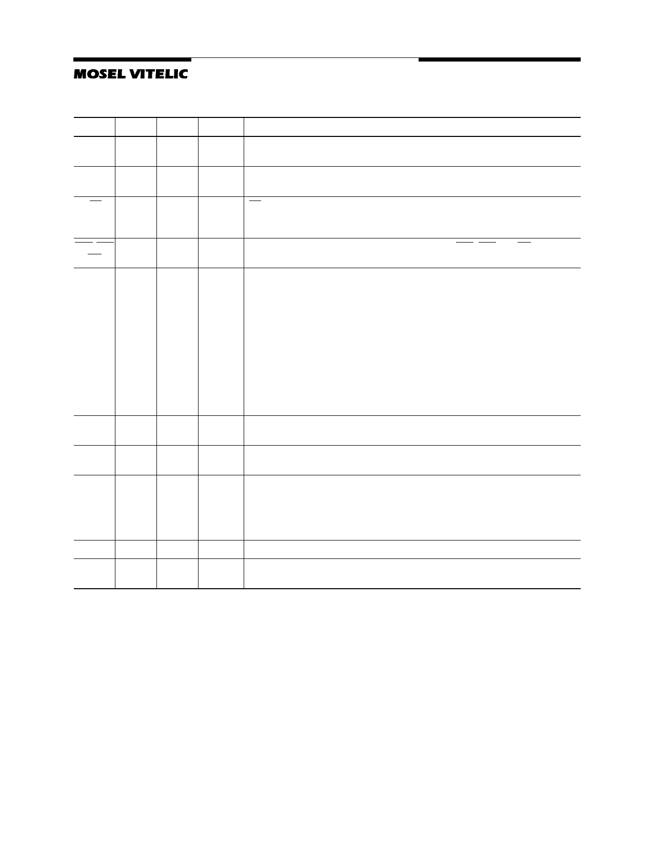
Signal Pin Description
Pin Type
CLK Input
CKE
Input
CS Input
RAS, CAS Input
WE
A0 - A11 Input
Signal Polarity
Function
Pulse
Positive The system clock input. All of the SDRAM inputs are sampled on the rising edge of the
Edge clock.
Level Active High Activates the CLK signal when high and deactivates the CLK signal when low, thereby
initiates either the Power Down mode or the Self Refresh mode.
Pulse
Active Low CS enables the command decoder when low and disables the command decoder when
high. When the command decoder is disabled, new commands are ignored but previous
operations continue.
Pulse Active Low When sampled at the positive rising edge of the clock, CAS, RAS, and WE define the
command to be executed by the SDRAM.
Level
— During a Bank Activate command cycle, A0-A12 defines the row address (RA0-RA12)
when sampled at the rising clock edge.
During a Read or Write command cycle, A0-An defines the column address (CA0-CAn)
when sampled at the rising clock edge.CAn depends from the SDRAM organization:
• 16M x 16 SDRAM CA0–CA8.
BA0,
BA1
DQx
LDQM
UDQM
Input
Input
Output
Input
VCC, VSS Supply
VCCQ
VSSQ
Supply
Level
In addition to the column address, A10(=AP) is used to invoke autoprecharge operation
at the end of the burst read or write cycle. If A10 is high, autoprecharge is selected and
BA0, BA1 defines the bank to be precharged. If A10 is low, autoprecharge is disabled.
During a Precharge command cycle, A10(=AP) is used in conjunction with BA0 and BA1
to control which bank(s) to precharge. If A10 is high, all four banks will BA0 and BA1 are
used to define which bank to precharge.
— Selects which bank is to be active.
Level
— Data Input/Output pins operate in the same manner as on conventional DRAMs.
Pulse
Active High The Data Input/Output mask places the DQ buffers in a high impedance state when sam-
pled high. In Read mode, DQM has a latency of two clock cycles and controls the output
buffers like an output enable. In Write mode, DQM has a latency of zero and operates as
a word mask by allowing input data to be written if it is low but blocks the write operation
if DQM is high.
Power and ground for the input buffers and the core logic.
— — Isolated power supply and ground for the output buffers to provide improved noise
immunity.
V54C3256164VBUC/T Rev. 1.1 February 2003
5
5 Page 
MOSEL VITELIC
V54C3256164VBUC/T
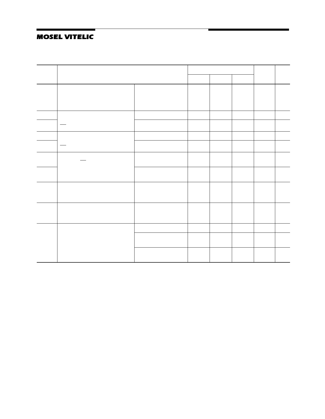
Operating Currents (TA = 0 to 70°C, VCC = 3.3V ± 0.3V)
(Recommended Operating Conditions unless otherwise noted)
Max.
Symbol Parameter & Test Condition
-6 -7 / -7PC -8PC Unit Note
ICC1
Operating Current
tRC = tRCMIN., tRC = tCKMIN.
Active-precharge command cycling,
without Burst Operation
1 bank operation
90 80 80 mA 7
ICC2P
ICC2PS
Precharge Standby Current
in Power Down Mode
CS =VIH, CKE≤ VIL(max)
ICC2N
ICC2NS
Precharge Standby Current
in Non-Power Down Mode
CS =VIH, CKE≥ VIL(max)
ICC3N
ICC3P
No Operating Current
tCK = min, CS = VIH(min)
bank ; active state ( 4 banks)
tCK = min.
tCK = Infinity
tCK = min.
tCK = Infinity
CKE ≥ VIH(MIN.)
CKE ≤ VIL(MAX.)
(Power down mode)
2 2 2 mA 7
1 1 1 mA 7
55 45 35 mA
5 5 5 mA
65 55 45 mA
10 10 10 mA
ICC4
Burst Operating Current
tCK = min
Read/Write command cycling
170 150 120 mA 7,8
ICC5
Auto Refresh Current
tCK = min
Auto Refresh command cycling
270 240 220 mA 7
ICC6 Self Refresh Current
Self Refresh Mode, CKE≤ 0.2V
L-version
(B component rev)
3 3 3 mA
1.0 1.0 1.0 mA
U-version
(B component rev)
0.6 0.6 0.6 mA
Notes:
7. These parameters depend on the cycle rate and these values are measured by the cycle rate under the minimum value of tCK and
tRC. Input signals are changed one time during tCK.
8. These parameter depend on output loading. Specified values are obtained with output open.
V54C3256164VBUC/T Rev. 1.1 February 2003
11
11 Page | ||
| Páginas | Total 30 Páginas | |
| PDF Descargar | [ Datasheet V54C3256164VBUC.PDF ] | |
Hoja de datos destacado
| Número de pieza | Descripción | Fabricantes |
| V54C3256164VBUC | LOW POWER 256Mbit SDRAM 3.3 VOLT/ 54-BALL SOC BGA 54-PIN TSOPII 16M X 16 | Mosel Vitelic Corp |
| V54C3256164VBUT | LOW POWER 256Mbit SDRAM 3.3 VOLT/ 54-BALL SOC BGA 54-PIN TSOPII 16M X 16 | Mosel Vitelic Corp |
| Número de pieza | Descripción | Fabricantes |
| SLA6805M | High Voltage 3 phase Motor Driver IC. |
Sanken |
| SDC1742 | 12- and 14-Bit Hybrid Synchro / Resolver-to-Digital Converters. |
Analog Devices |
|
DataSheet.es es una pagina web que funciona como un repositorio de manuales o hoja de datos de muchos de los productos más populares, |
| DataSheet.es | 2020 | Privacy Policy | Contacto | Buscar |
