|
|
|
PDF VSC7212RG Data sheet ( Hoja de datos )
| Número de pieza | VSC7212RG | |
| Descripción | Gigabit Interconnect Chip | |
| Fabricantes | ETC | |
| Logotipo | ||
Hay una vista previa y un enlace de descarga de VSC7212RG (archivo pdf) en la parte inferior de esta página. Total 34 Páginas | ||
|
No Preview Available !
VIITTEESSSSEE
SEEMMIICCOONNDDUUCCTTOORRCCOORPROPROARTAIOTNION
Preliminary Data Sheet
VSC7212
Gigabit Interconnect Chip
Features
• ANSI X3T11 Compliant Fibre Channel and IEEE
802.3z Compliant Gigabit Ethernet Transceiver
• Over 2Gb/s Duplex Raw Data Rate
• Redundant PECL Tx Outputs and Rx Inputs
• 8B/10B Encoder/Decoder, Optional Encoder/
Decoder Bypass Operation
• “ASIC-FriendlyTM” Timing Options for Transmit-
ter Parallel Input Data
• Elastic Buffer for Chip-to-Chip Cable Deskewing
• Tx/Rx Rate Matching via IDLE Insertion/Deletion
• Compatible with VSC7211, VSC7214 and
VSC7216
• Received Data Aligned to Local REFCLK or to
Recovered Clock
• PECL Rx Signal Detect and Cable Equalization
• Serial Tx-to-Rx and Parallel Rx-to-Tx Internal
Loopback Modes
• Clock Multiplier Generates Baud Rate Clock
• Automatic Lock-to-Reference
• JTAG Boundary Scan Support for TTL I/O
• Built-In Self Test
• 3.3V Supply, 1.0 W
• 100-pin, 14mm TQFP package
General Description
The VSC7212 is an 8-bit parallel-to-serial and serial-to-parallel transceiver chip used for high bandwidth
interconnection between busses, backplanes, or other subsystems. A Fibre Channel and Gigabit Ethernet
compliant transceiver provides up to 2.18Gb/s of duplex raw data transfer. The VSC7212 can operate at a
maximum data transfer rate of 1088Mb/s (8 bits at 136MHz) or a minimum rate of 784Mb/s (8 bits at 98MHz).
The VSC7212 contains an 8B/10B encoder, serializer, de-serializer, 8B/10B decoder and elastic buffer which
provide the user with a simple interface for transferring data serially and recovering it on the receive side. The
device can also be configured to operate as a non-encoded 10-bit transceiver with redundant I/O.
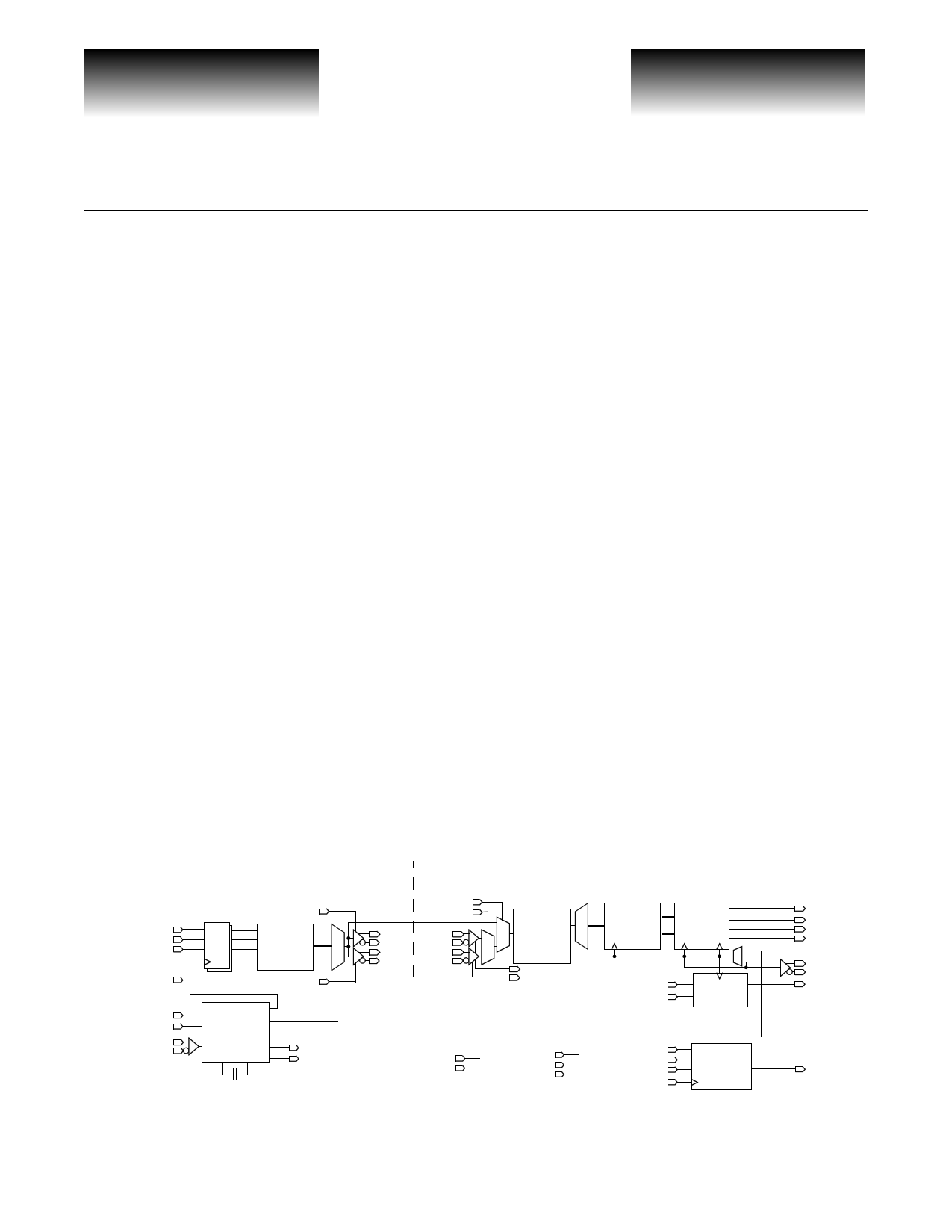
VSC7212 Block Diagram
T(7:0)
C/D
WSEN
KCHAR
TRANSMITTER
88
DQ
PTXEN
8B/10B 10
Encode
RTXEN
LBTX
PTX+
PTX-
RTX+
RTX-
LBEN(1:0)
RXP/R
PRX+
PRX-
RRX+
RRX-
DUAL
TBC
REFCLKP
REFCLKN
x20/x10
Clock Gen
CAP0 CAP1
Tx Clock
REFCLK
TBERR
REFOUT
TMODE(2:0)
RMODE(1:0)
RECEIVER
Clk/Data
Recovery
PSDET
RSDET
8
10 8B/10B 8 Elastic
Decode 3 Buffer
WSI
FLOCK
Channel
Align
RESETN
ENDEC
BIST
TRSTN
TMS
TDI
TCK
JTAG
Boundary
Scan
R(7:0)
IDLE
KCH
ERR
RCLK
RCLKN
WSO
TDO
G52268-0, Rev 3.3
04/10/01
© VITESSE SEMICONDUCTOR CORPORATION • 741 Calle Plano • Camarillo, CA 93012
Tel: (800)-VITESSE • FAX: (805) 987-5896 • Email: [email protected]
Internet: www.vitesse.com
Page 1
1 page 
VIITTEESSSSEE
SEEMMIICCOONNDDUUCCTTOORRCCOORPROPROARTAIOTNION
Preliminary Data Sheet
VSC7212
Gigabit Interconnect Chip
8B/10B Encoder
The VSC7212 contains an 8B/10B encoder which translates the 8-bit input data on T(7:0) into a 10-bit
encoded data character. A C/D input is also provided which, along with KCHAR, allow the transmission of
special Fibre Channel Kxx.x characters (see Table 2). Note that KCHAR is a static input, and does NOT have
the same input timing as T(7:0), C/D and WSEN. Normally C/D is LOW in order to transmit data. If C/D is
HIGH and KCHAR is LOW, then a Fibre Channel defined IDLE Character (K28.5 = ‘0011111010’ or
‘1100000101’ depending on disparity) is transmitted and T(7:0) is ignored. If C/D is HIGH and KCHAR is
HIGH, a Kxx.x character is transmitted as determined by the data on T(7:0) (see Table 3). Data patterns other
than those defined in Table 3 produce undefined 10B encodings.
Table 2: Transmit Data Controls
WSEN
0
0
0
1
C/D KCHAR
Encoded 10-bit Output
0 X Data Character
1 0 IDLE Character (K28.5)
1 1 Special Kxx.x Character
X X 16-Character Word Sync Sequence
Table 3: Special Characters (Selected when C/D and KCHAR are HIGH)
Code
K28.0
K28.1
K28.2
K28.3
K28.4
K28.5
T(7:0)
000 11100
001 11100
010 11100
011 11100
100 11100
101 11100
Comment
User Defined
User Defined
User Defined
User Defined
User Defined
IDLE
Code
K28.6
K28.7
K23.7
K27.7
K29.7
K30.7
T(7:0)
110 11100
111 11100
111 10111
111 11011
111 11101
111 11110
Comment
User Defined
Test Only
User Defined
User Defined
User Defined
User Defined
Encoder Bypass Mode
When ENDEC is LOW the 8B/10B encoder is bypassed and a 10-bit input character T(7:0) is serialized
onto PTX/RTX with bit T0 is transmitted first. The C/D input becomes T8, and WSEN becomes T9. The
KCHAR input becomes ENCDET which is not used in the transmitter, but when HIGH, enables “Comma”
detection in the receiver. Refer to the “Decoder Bypass Mode” section for a description of this mode of
operation in the receiver. The latency through the transmitter is reduced by one character time when ENDEC is
LOW. This mode of operation is similar to a 10-bit interface commonly found in serializer/deserializers for the
Fibre Channel (e.g., VSC7125) and Gigabit Ethernet markets (e.g., VSC7135).
G52268-0, Rev 3.3
04/10/01
© VITESSE SEMICONDUCTOR CORPORATION • 741 Calle Plano • Camarillo, CA 93012
Internet: www.vitesse.com
Page 5
5 Page 
VIITTEESSSSEE
SEEMMIICCOONNDDUUCCTTOORRCCOORPROPROARTAIOTNION
Preliminary Data Sheet
VSC7212
Gigabit Interconnect Chip
If RMODE1 is LOW and if the transmitting device’s REFCLK is not precisely frequency-locked to a
receiver’s REFCLK, then the channel’s elastic buffer will tend to gradually fill or empty as the recovered clock
(which is by definition frequency-locked to the transmitter’s REFCLK) steadily drifts in phase relative to the
word clock. In order to accommodate frequency differences between a transmitter’s REFCLK and the receiver’s
REFCLK, the VSC7212 can automatically perform “rate matching” by either deleting or duplicating IDLE
characters. FLOCK must be LOW and WSI must be connected to WSO to enable rate matching. It is the user’s
responsibility to ensure that the frequency at which IDLEs are transmitted accommodates the frequency
differences, if any, in their system architecture. Not meeting the IDLE density requirements described below
may result in Underrun/Overrun Errors.
The elastic buffer is designed to allow a maximum phase drift of +2 or -2 serial clock bit times between re-
synchronizations, which sets a limit on the maximum data “packet” length allowed between IDLEs. This
maximum packet length depends on the frequency difference between the transmitting and receiving devices
REFCLKs. Let ∆φ represent phase drift in bit times, and let 2π represent one full 10-bit character of phase
drift. Limiting phase drift to two bit times means the following inequality must be satisfied:
(1) ∆φ ≤ (0.2 × 2π)
Let L be the number of 10-bit characters transmitted, and let Df be the frequency offset in ppm. The total
phase drift in bit times is given by:
(2) ∆φ = (∆f ⁄ 106) × 2πL
A simple expression for maximum packet length as a function of frequency offset is derived by substituting
(2) in (1) and solving for L:
(3) L ≤ (0.2 × 10⁶) ⁄ ∆f
As an example, if the frequency offset is 200ppm, then the maximum packet length should not be more than
1K bytes. To increase the maximum packet length L, decrease the frequency offset Df. Note that if only one
K28.5 is transmitted between “packets” of data, it might be dropped during compensation for phase drift. If the
user must have at least one K28.5 between these two packets, then two K28.5s must be transmitted.
Using Multiple VSC7212s in Parallel
Multiple VSC7212s and VSC7216s can be used in parallel to form wider bus widths. In order for chip-to-
chip word alignment to function correctly across multiple devices, each transmit channel’s input data must be
transmitted synchronously to a common REFCLK or TBC, and each receiver’s output data must also be aligned
to a common REFCLK. This requires that all transmitting devices use either the same or identical REFCLKs,
and that TMODE(2:0)=000 (inputs timed to REFCLK) or TMODE(2:0)=1X0 (inputs timed to TBC). If inputs
are timed to TBC, then all transmitting devices must use either the same or identical TBCs. Since all receive
channels must use a common word clock, the receiving devices must also use the same or identical REFCLKs
and it must be selected as the word clock for all receive channels (RMODE(1:0)=0X).
G52268-0, Rev 3.3
04/10/01
© VITESSE SEMICONDUCTOR CORPORATION • 741 Calle Plano • Camarillo, CA 93012
Internet: www.vitesse.com
Page 11
11 Page | ||
| Páginas | Total 34 Páginas | |
| PDF Descargar | [ Datasheet VSC7212RG.PDF ] | |
Hoja de datos destacado
| Número de pieza | Descripción | Fabricantes |
| VSC7212RG | Gigabit Interconnect Chip | ETC |
| Número de pieza | Descripción | Fabricantes |
| SLA6805M | High Voltage 3 phase Motor Driver IC. |
Sanken |
| SDC1742 | 12- and 14-Bit Hybrid Synchro / Resolver-to-Digital Converters. |
Analog Devices |
|
DataSheet.es es una pagina web que funciona como un repositorio de manuales o hoja de datos de muchos de los productos más populares, |
| DataSheet.es | 2020 | Privacy Policy | Contacto | Buscar |