|
|
|
PDF X28LC512J-25 Data sheet ( Hoja de datos )
| Número de pieza | X28LC512J-25 | |
| Descripción | 3.3 Volt/ Byte Alterable E2PROM | |
| Fabricantes | Xicor | |
| Logotipo | ||
Hay una vista previa y un enlace de descarga de X28LC512J-25 (archivo pdf) en la parte inferior de esta página. Total 19 Páginas | ||
|
No Preview Available !
X28LC512/X28LC513
512K
X28LC512/X28LC513
3.3 Volt, Byte Alterable E2PROM
64K x 8 Bit
FEATURES
• Low VCC Operation: VCC = 3.3V ±10%
• Access Time: 150ns
• Simple Byte and Page Write
—Self-Timed
—No Erase Before Write
—No Complex Programming Algorithms
—No Overerase Problem
• Low Power CMOS:
—Active: 25mA
—Standby: 150µA
• Software Data Protection
—Protects Data Against System Level
Inadvertant Writes
• High Speed Page Write Capability
• Highly Reliable Direct Write™ Cell
—Endurance: 10,000 Write Cycles
—Data Retention: 100 Years
• Early End of Write Detection
—DATA Polling
—Toggle Bit Polling
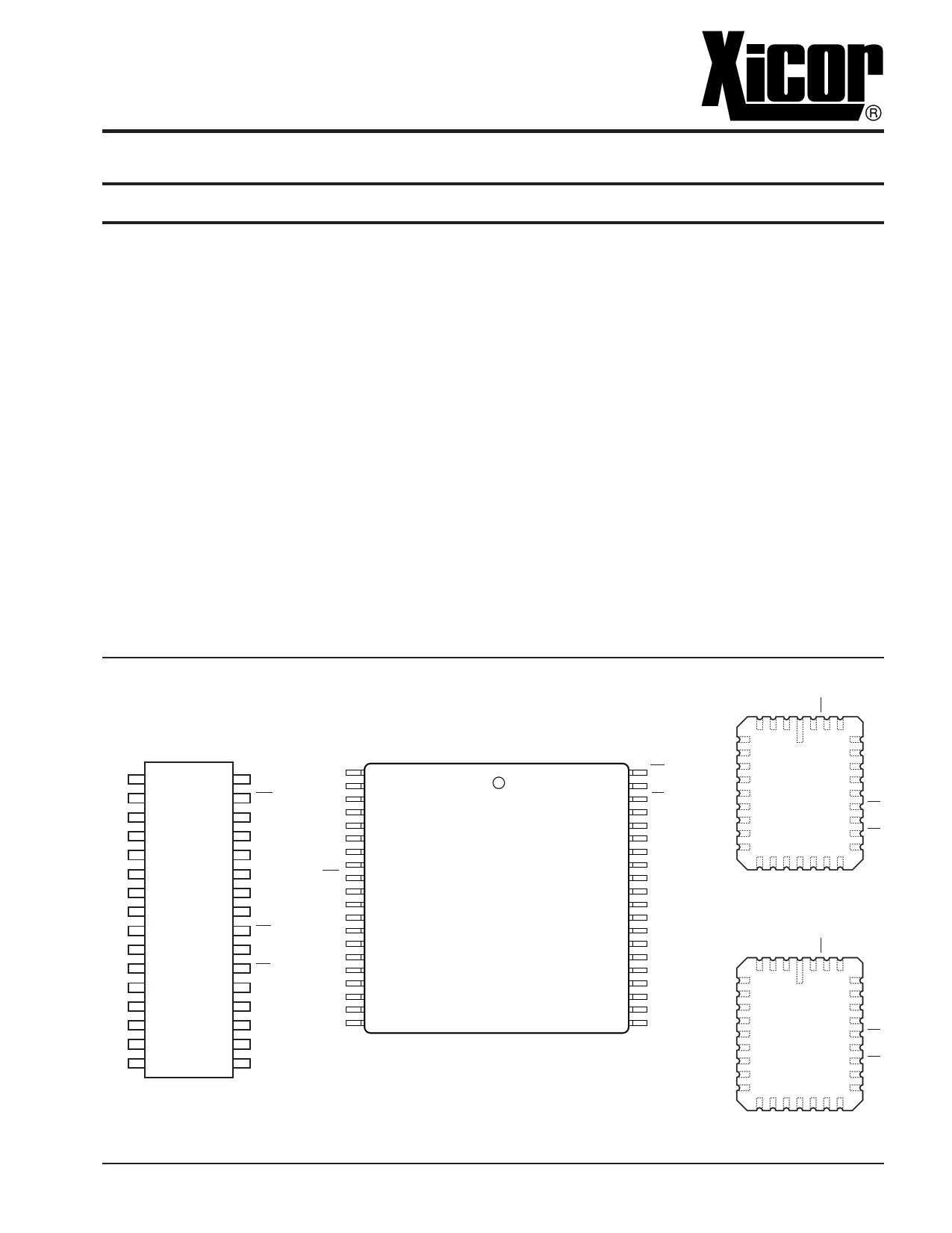
PIN CONFIGURATIONS
• Two PLCC and LCC Pinouts
—X28LC512
—X28LC010 E2PROM Pin Compatible
—X28LC513
—Compatible with Lower Density E2PROMs
DESCRIPTION
The X28LC512/513 is a low-power 64K x 8 E2PROM,
fabricated with Xicor’s proprietary, high performance,
floating gate CMOS technology. The X28LC512/513
features the JEDEC approved pinout for bytewide memo-
ries, compatible with industry standard EPROMS.
The X28LC512/513 supports a 128-byte page write
operation, effectively providing a 39µs/byte write cycle
and enabling the entire memory to be written in less than
2.5 seconds. The X28LC512/513 also features DATA
Polling and Toggle Bit Polling, system software support
schemes used to indicate the early completion of a write
cycle. In addition, the X28LC512/513 supports the Soft-
ware Data Protection option.
PLCC
NC
NC
A15
A12
A7
A6
A5
A4
A3
A2
A1
A0
I/O0
I/O1
I/O2
VSS
PLASTIC DIP
1 32
2 31
3 30
4 29
5 28
6 27
7 26
8 25
X28LC512
9 24
10 23
11 22
12 21
13 20
14 19
15 18
16 17
VCC
WE
NC
A14
A13
A8
A9
A11
OE
A10
CE
I/O7
I/O6
I/O5
I/04
I/O3
3005 ILL F02.1
A11
A9
A8
A13
A14
NC
NC
NC
WE
VCC
NC
NC
NC
NC
A15
A12
A7
A6
A5
A4
1
2
3
4
5
6
7
8
9
10
11
12
13
14
15
16
17
18
19
20
© Xicor, Inc. 1991, 1995, 1996 Patents Pending
3005-3.2 8/5/97 T2/C0/D0 EW
TSOP
X28LC512
1
40 OE
39 A10
38 CE
37 I/O7
36 I/O6
35 I/O5
34 I/O4
33 I/O3
32 NC
31 NC
30 VSS
29 NC
28 NC
27 I/O2
26 I/O1
25 I/O0
24 A0
23 A1
22 A2
21 A3
3005 ILL F22.2
30
A7
A6
5 4 3 2 32 31 29
6 1 28
A14
A13
A5 7
27 A8
A4
A3
8 26
9
X28LC512
(TOP VIEW)
25
A9
A11
A2 10
24 OE
A1 11
23 A10
A0 12
22 CE
I/O0
13
14
15 16 17 18 19 20 21
I/O7
3005 ILL F03
PLCC
30
A6
A5
5 4 3 2 32 31 29
6 1 28
A8
A9
A4 7
27 A11
A3
A2
8 26
9
X28LC513
(TOP VIEW)
25
NC
OE
A1 10
24 A10
A0 11
23 CE
NC 12
22 I/O7
I/O0
13
14
15 16 17 18 19 20 21
I/O6
3005 ILL F04.1
Characteristics subject to change without notice
1 page 
X28LC512/X28LC513
The Toggle Bit I/O6
Figure 3a. Toggle Bit Bus Sequence
LAST
WE WRITE
CE
OE
I/O6
VOH
*
VOL
* Beginning and ending state of I/O6 will vary.
Figure 3b. Toggle Bit Software Flow
LAST WRITE
LOAD ACCUM
FROM ADDR n
COMPARE
ACCUM WITH
ADDR n
HIGH Z
*
X28LC512
READY
3005 ILL F14
The Toggle Bit can eliminate the software housekeeping
chore of saving and fetching the last address and data
written to a device in order to implement DATA Polling.
This can be especially helpful in an array comprised of
multiple X28LC512/513 memories that is frequently
updated. Toggle Bit Polling can also provide a method
for status checking in multiprocessor applications. The
timing diagram in Figure 3a illustrates the sequence of
events on the bus. The software flow diagram in Figure
3b illustrates a method for polling the Toggle Bit.
COMPARE
OK?
YES
X28LC512
READY
NO
3005 ILL F15
5
5 Page 
X28LC512/X28LC513
POWER-UP TIMING
Symbol
tPUR(2)
tPUW(2)
Parameter
Power-up to Read Operation
Power-up to Write Operation
CAPACITANCE TA = +25°C, f = 1MHz, VCC = 3.3V
Symbol
Parameter
CI/O(2)
CIN(2)
Input/Output Capacitance
Input Capacitance
ENDURANCE AND DATA RETENTION
Parameter
Min.
Endurance
Data Retention
10,000
100
Max.
100
5
Max.
10
10
Units
pF
pF
Max.
A.C. CONDITIONS OF TEST
Input Pulse Levels
0V to 3V
Input Rise and
Fall Times
Input and Output
Timing Levels
10ns
1.5V
3856 PGM T07.1
MODE SELECTION
CE OE WE
L LH
L HL
H XX
X LX
X XH
Mode
Read
Write
Standby and
Write Inhibit
Write Inhibit
Write Inhibit
EQUIVALENT A.C. LOAD CIRCUIT
SYMBOL TABLE
Units
µs
ms
3005 PGM T05
Test Conditions
VI/O = 0V
VIN = 0V
3005 PGM T06.1
Units
Cycles per Byte
Years
3005 PGM T11
I/O
DOUT
DIN
High Z
Power
Active
Active
Standby
——
——
3005 PGM T08
5V
2.66KΩ
OUTPUT
4.46KΩ
30pF
3005 ILL F21.3
Note: (2) This parameter is periodically sampled and not 100%
tested.
WAVEFORM INPUTS
OUTPUTS
Must be
steady
May change
from LOW
to HIGH
May change
from HIGH
to LOW
Don’t Care:
Changes
Allowed
N/A
Will be
steady
Will change
from LOW
to HIGH
Will change
from HIGH
to LOW
Changing:
State Not
Known
Center Line
is High
Impedance
11
11 Page | ||
| Páginas | Total 19 Páginas | |
| PDF Descargar | [ Datasheet X28LC512J-25.PDF ] | |
Hoja de datos destacado
| Número de pieza | Descripción | Fabricantes |
| X28LC512J-20 | 3.3 Volt/ Byte Alterable E2PROM | Xicor |
| X28LC512J-25 | 3.3 Volt/ Byte Alterable E2PROM | Xicor |
| Número de pieza | Descripción | Fabricantes |
| SLA6805M | High Voltage 3 phase Motor Driver IC. |
Sanken |
| SDC1742 | 12- and 14-Bit Hybrid Synchro / Resolver-to-Digital Converters. |
Analog Devices |
|
DataSheet.es es una pagina web que funciona como un repositorio de manuales o hoja de datos de muchos de los productos más populares, |
| DataSheet.es | 2020 | Privacy Policy | Contacto | Buscar |