|
|
|
PDF X9251 Data sheet ( Hoja de datos )
| Número de pieza | X9251 | |
| Descripción | Quad Digitally-Controlled (XDCP) Potentiometer | |
| Fabricantes | Xicor | |
| Logotipo | ||
Hay una vista previa y un enlace de descarga de X9251 (archivo pdf) en la parte inferior de esta página. Total 25 Páginas | ||
|
No Preview Available !
APPLICATION NOTES AND DEVELOPMENT SYSTEM
AVAILABLE
AN99 • AN115 • AN124 •AN133 • AN134 • AN135
Single Supply / Low Power / 256-tap / SPI bus
X9251
Quad Digitally-Controlled (XDCPTM) Potentiometer
FEATURES
• Four potentiometers in one package
• 256 resistor taps–0.4% resolution
• SPI Serial Interface for write, read, and transfer
operations of the potentiometer
• Wiper resistance: 100Ω typical @ VCC = 5V
• 4 Non-volatile data registers for each
potentiometer
• Non-volatile storage of multiple wiper positions
• Standby current < 5µA max
• VCC: 2.7V to 5.5V Operation
• 50KΩ, 100KΩ versions of total resistance
• 100 yr. data retention
• Single supply version of X9250
• Endurance: 100,000 data changes per bit per
register
• 24-lead SOIC, 24-lead TSSOP, 24-lead CSP
(Chip Scale Package)
• Low power CMOS
DESCRIPTION
The X9251 integrates four digitally controlled potentio-
meters (XDCP) on a monolithic CMOS integrated
circuit.
The digitally controlled potentiometers are imple-
mented with a combination of resistor elements and
CMOS switches. The position of the wipers are
controlled by the user through the SPI bus interface.
Each potentiometer has associated with it a volatile
Wiper Counter Register (WCR) and four non-volatile
Data Registers that can be directly written to and read
by the user. The content of the WCR controls the
position of the wiper. At power-up, the device recalls
the content of the default Data Registers of each DCP
(DR00, DR10, DR20, and DR30) to the corresponding
WCR.
The XDCP can be used as a three-terminal
potentiometer or as a two terminal variable resistor in
a wide variety of applications including control,
parameter adjustments, and signal processing.
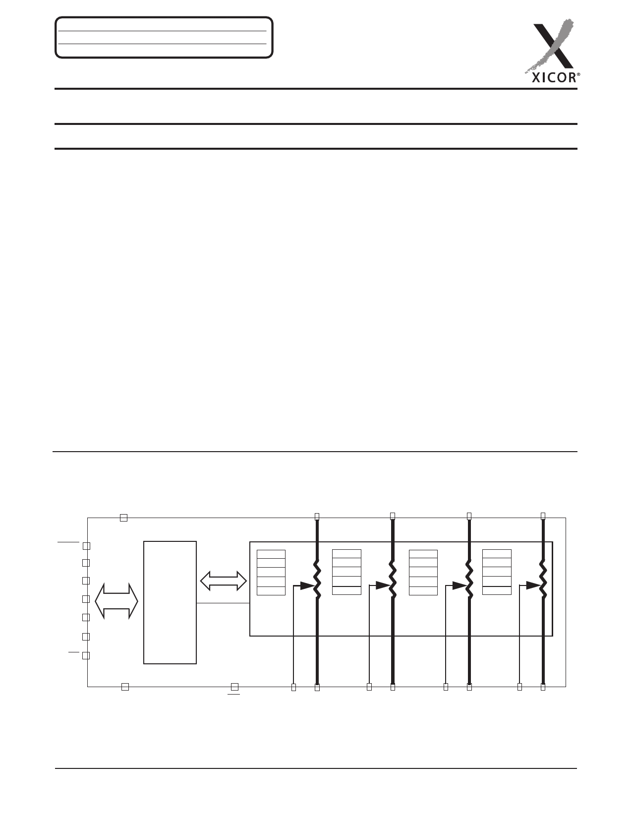
FUNCTIONAL DIAGRAM
VCC
RH0
RH1
RH2
RH3
HOLD
A1
A0
SO
SI
SCK
CS
SPI
Interface
POWER UP,
INTERFACE
CONTROL
AND
STATUS
WCR0
DR00
DR01
DR02
DR03
DCP0
WCR1
DR10
DR11
DR12
DR13
DCP1
WCR2
DR20
DR21
DR22
DR23
DCP2
WCR3
DR30
DR31
DR32
DR33
DCP3
VSS
WP
RW0 RL0
RW1 RL1
RW2 RL2
RW3 RL3
REV 1.3.3 2/10/04
www.xicor.com
Characteristics subject to change without notice. 1 of 25
1 page 
X9251
PIN DESCRIPTIONS
Bus Interface Pins
SERIAL OUTPUT (SO)
SO is a serial data output pin. During a read cycle,
data is shifted out on this pin. Data is clocked out by
the falling edge of the serial clock.
SERIAL INPUT (SI)
SI is the serial data input pin. All opcodes, byte
addresses and data to be written to the device
registers are input on this pin. Data is latched by the
rising edge of the serial clock.
SERIAL CLOCK (SCK)
The SCK input is used to clock data into and out of the
X9251.
HOLD (HOLD)
HOLD is used in conjunction with the CS pin to select
the device. Once the part is selected and a serial
sequence is underway, HOLD may be used to pause
the serial communication with the controller without
resetting the serial sequence. To pause, HOLD must
be brought LOW while SCK is LOW. To resume
communication, HOLD is brought HIGH, again while
SCK is LOW. If the pause feature is not used, HOLD
should be held HIGH at all times.
DEVICE ADDRESS (A1–A0)
The address inputs are used to set the two least
significant bits of the slave address. A match in the
slave address serial data stream must be made with
the address input in order to initiate communication
with the X9251. Device pins A1-A0 must be tie to a
logic level which specify the internal address of the
device, see Figures 2, 3, 4, 5 and 6.
CHIP SELECT (CS)
When CS is HIGH, the X9251 is deselected and the
SO pin is at high impedance, and (unless an internal
write cycle is underway) the device is in the standby
state. CS LOW enables the X9251, placing it in the
active power mode. It should be noted that after a
power-up, a HIGH to LOW transition on CS is required
prior to the start of any operation.
Potentiometer Pins
RH, RL
The RH and RL pins are equivalent to the terminal
connections on a mechanical potentiometer. Since
there are 4 potentiometers, there are 4 sets of RH and
RL such that RH0 and RL0 are the terminals of DCP0
and so on.
RW
The wiper pin are equivalent to the wiper terminal of a
mechanical potentiometer. Since there are 4
potentiometers, there are 4 sets of RW such that RW0
is the terminals of DCP0 and so on.
Supply Pins
SYSTEM SUPPLY VOLTAGE (VCC) AND SUPPLY GROUND (VSS)
The VCC pin is the system supply voltage. The VSS pin
is the system ground.
Other Pins
NO CONNECT
No connect pins should be left floating. This pins are
used for Xicor manufacturing and testing purposes.
HARDWARE WRITE PROTECT INPUT (WP)
The WP pin when LOW prevents non-volatile writes to
the Data Registers.
REV 1.3.3 2/10/04
www.xicor.com
Characteristics subject to change without notice. 5 of 25
5 Page 
X9251
Figure 2. Two-Byte Instruction Sequence
CS
SCK
SI
0 1 0 10
ID3 ID2 ID1 ID0 0
Device ID
0
0 A1 A0 I3 I2 I1 I0 RB RA P1 P0
Internal
Address
Instruction
Opcode
Register DCP/WCR
Address Address
Figure 3. Three-Byte Instruction Sequence SPI Interface; Write Case
CS
SCK
SI 0 1 0 1 0 0
ID3 ID2 ID1 ID0 0 0 A1 A0
I3 I2 I1 I0 RB RA P1 P0
D7 D6 D5 D4 D3 D2 D1 D0
Device ID
Internal
Address
Instruction
Opcode
Register DCP/WCR
Address Address
Data for WCR[7:0] or DR[7:0]
Figure 4. Three-Byte Instruction Sequence SPI Interface, Read Case
CS
SCK
SI 0 1 0 1 0 0
ID3 ID2 ID1 ID0 0 0 A1 A0 I3 I2 I1 I0 RB RA P1 P0
XXXX XXXX
Don’t Care
Device ID
Internal
Address
Instruction RegisterDCP/WCR
Opcode
Address Address
S0
D7 D6 D5 D4 D3 D2 D1 D0
WCR[7:0]
or
Data Register Bit [7:0]
REV 1.3.3 2/10/04
www.xicor.com
Characteristics subject to change without notice. 11 of 25
11 Page | ||
| Páginas | Total 25 Páginas | |
| PDF Descargar | [ Datasheet X9251.PDF ] | |
Hoja de datos destacado
| Número de pieza | Descripción | Fabricantes |
| X9250 | Quad Digitally Controlled Potentiometers (XDCP) | Xicor |
| X9250 | Quad Digitally Controlled Potentiometers | Intersil Corporation |
| X9251 | Quad Digitally-Controlled (XDCP) Potentiometer | Xicor |
| X9251 | Quad Digitally-Controlled Potentiometer | Intersil Corporation |
| Número de pieza | Descripción | Fabricantes |
| SLA6805M | High Voltage 3 phase Motor Driver IC. |
Sanken |
| SDC1742 | 12- and 14-Bit Hybrid Synchro / Resolver-to-Digital Converters. |
Analog Devices |
|
DataSheet.es es una pagina web que funciona como un repositorio de manuales o hoja de datos de muchos de los productos más populares, |
| DataSheet.es | 2020 | Privacy Policy | Contacto | Buscar |