|
|
PDF K4S161622H-TC55 Data sheet ( Hoja de datos )
| Número de pieza | K4S161622H-TC55 | |
| Descripción | 16Mb H-die SDRAM Specification | |
| Fabricantes | Samsung semiconductor | |
| Logotipo | ||
Hay una vista previa y un enlace de descarga de K4S161622H-TC55 (archivo pdf) en la parte inferior de esta página. Total 11 Páginas | ||
|
No Preview Available !
SDRAM 16Mb H-die(x16)
CMOS SDRAM
16Mb H-die SDRAM Specification
Revision 1.5
August 2004
Samsung Electronics reserves the right to change products or specification without notice.
Rev. 1.5 August 2004
1 page 
SDRAM 16Mb H-die(x16)
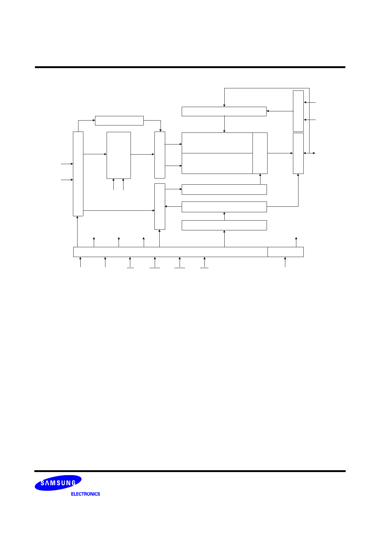
FUNCTIONAL BLOCK DIAGRAM
Bank Select
CMOS SDRAM
Data Input Register
LWE
LDQM
512K x 16
CLK
ADD
512K x 16
Column Decoder
LCKE
LRAS
LCBR
LWE
LCAS
Latency & Burst Length
Programming Register
LWCBR
Timing Register
DQi
LDQM
CLK
CKE
CS
RAS
CAS
WE
L(U)DQM
* Samsung Electronics reserves the right to change products or specification without notice.
Rev. 1.5 August 2004
5 Page 
SDRAM 16Mb H-die(x16)
CMOS SDRAM
SIMPLIFIED TRUTH TABLE
COMMAND
CKEn-1 CKEn CS RAS CAS WE DQM BA A10/AP A9~ A0 Note
Register
Mode Register Set
H X LL LLX
OP CODE
1, 2
Auto Refresh
H3
H
LL
LHX
X
Entry
L
3
Refresh
Self
Refresh
Exit
LH HH
LH
X
X
3
HX
XX
3
Bank Active & Row Addr.
H X L L H H X V Row Address
Read &
Auto Precharge Disable
Column Address Auto Precharge Enable
H
X LH LHXV
L
Column
4
H Address 4, 5
Write &
Auto Precharge Disable
Column Address Auto Precharge Enable
H
X LH L L XV
L
Column
4
H Address 4, 5
Burst Stop
H X LH HL X X 6
Precharge
Bank Selection
Both Banks
VL
H X LL HLX
XH
X
Clock Suspend or
Active Power Down
Entry
Exit
HX
XX
HL
X
LV
VV
L H XX XX X
X
Precharge Power Down Mode
Entry
Exit
HX
XX
HL
X
LH HH
HX
XX
LH
X
LV
VV
X
DQM
H X VX7
No Operation Command
HX
XX
HX
X
LH HH
X
(V=Valid, X=Don′t Care, H=Logic High, L=Logic Low)
Note : 1. OP Code : Operand Code
A0 ~ A10/AP, BA : Program keys. (@MRS)
2. MRS can be issued only at both banks precharge state.
A new command can be issued after 2 clock cycle of MRS.
3. Auto refresh functions are as same as CBR refresh of DRAM.
The automatical precharge without row precharge command is meant by "Auto".
Auto/self refresh can be issued only at both banks precharge state.
4. BA : Bank select address.
If "Low" at read, write, row active and precharge, bank A is selected.
If "High" at read, write, row active and precharge, bank B is selected.
If A10/AP is "High" at row precharge, BA is ignored and both banks are selected.
5. During burst read or write with auto precharge, new read/write command can not be issued.
Another bank read/write command can be issued after the end of burst.
New row active of the assoiated bank can be issued at tRP after the end of burst.
6. Burst stop command is valid at every burst length.
7. DQM sampled at positive going edge of a CLK masks the data-in at the very CLK (Write DQM latency is 0),
but makes Hi-Z state the data-out of 2 CLK cycles after. (Read DQM latency is 2)
Rev. 1.5 August 2004
11 Page | ||
| Páginas | Total 11 Páginas | |
| PDF Descargar | [ Datasheet K4S161622H-TC55.PDF ] | |
Hoja de datos destacado
| Número de pieza | Descripción | Fabricantes |
| K4S161622H-TC55 | 16Mb H-die SDRAM Specification | Samsung semiconductor |
| Número de pieza | Descripción | Fabricantes |
| SLA6805M | High Voltage 3 phase Motor Driver IC. |
Sanken |
| SDC1742 | 12- and 14-Bit Hybrid Synchro / Resolver-to-Digital Converters. |
Analog Devices |
|
DataSheet.es es una pagina web que funciona como un repositorio de manuales o hoja de datos de muchos de los productos más populares, |
| DataSheet.es | 2020 | Privacy Policy | Contacto | Buscar |
