|
|
PDF INA103 Data sheet ( Hoja de datos )
| Número de pieza | INA103 | |
| Descripción | Low Noise/ Low Distortion INSTRUMENTATION AMPLIFIER | |
| Fabricantes | Burr-Brown Corporation | |
| Logotipo |  |
|
Hay una vista previa y un enlace de descarga de INA103 (archivo pdf) en la parte inferior de esta página. Total 12 Páginas | ||
|
No Preview Available !
®
INA103
INA103
INA103
Low Noise, Low Distortion
INSTRUMENTATION AMPLIFIER
FEATURES
q LOW NOISE: 1nV/√Hz
q LOW THD+N: 0.0009% at 1kHz, G = 100
q HIGH GBW: 100MHz at G = 1000
q WIDE SUPPLY RANGE: ±9V to ±25V
q HIGH CMRR: >100dB
q BUILT-IN GAIN SETTING RESISTORS:
G = 1, 100
q UPGRADES AD625
APPLICATIONS
q HIGH QUALITY MICROPHONE PREAMPS
(REPLACES TRANSFORMERS)
q MOVING-COIL PREAMPLIFIERS
q DIFFERENTIAL RECEIVERS
q AMPLIFICATION OF SIGNALS FROM:
Strain Gages (Weigh Scale Applications)
Thermocouples
Bridge Transducers
DESCRIPTION
The INA103 is a very low noise, low distortion mono-
lithic instrumentation amplifier. Its current-feedback
circuitry achieves very wide bandwidth and excellent
dynamic response. It is ideal for low-level audio
signals such as balanced low-impedance microphones.
The INA103 provides near-theoretical limit noise per-
formance for 200Ω source impedances. Many indus-
trial applications also benefit from its low noise and
wide bandwidth.
Unique distortion cancellation circuitry reduces dis-
tortion to extremely low levels, even in high gain. Its
balanced input, low noise and low distortion provide
superior performance compared to transformer-coupled
microphone amplifiers used in professional audio
equipment.
The INA103’s wide supply voltage (±9 to ±25V) and
high output current drive allow its use in high-level
audio stages as well. A copper lead frame in the plastic
DIP assures excellent thermal performance.
The INA103 is available in 16-pin plastic DIP and
SOL-16 surface-mount packages. Commercial and In-
dustrial temperature range models are available.
Offset Offset
–Gain Drive Null Null
12 3 4
–Input 16
–Gain Sense 15
–RG 13
G = 100 14
+RG 6
+Gain Sense 2
+Input 1
+
A1
–
3kΩ
60.6Ω
3kΩ
–
A2
+
6kΩ
6kΩ
6kΩ
11 Sense
–
A3 10 Output
+
6kΩ
7 Ref
5
+Gain Drive
9
V+
8
V–
International Airport Industrial Park • Mailing Address: PO Box 11400, Tucson, AZ 85734 • Street Address: 6730 S. Tucson Blvd., Tucson, AZ 85706 • Tel: (520) 746-1111 • Twx: 910-952-1111
Internet: http://www.burr-brown.com/ • FAXLine: (800) 548-6133 (US/Canada Only) • Cable: BBRCORP • Telex: 066-6491 • FAX: (520) 889-1510 • Immediate Product Info: (800) 548-6132
©1990 Burr-Brown Corporation
PDS-11016H
INA103Printed in U.S.A. March, 1998
®
1 page 
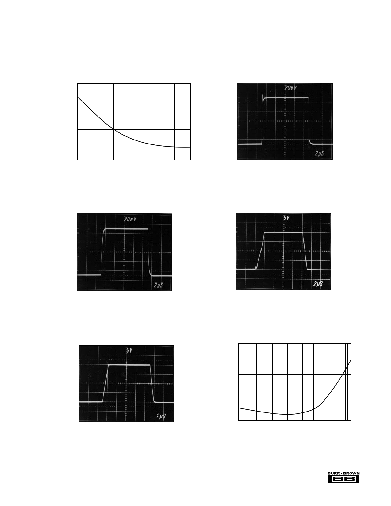
TYPICAL PERFORMANCE CURVES (CONT)
At TA = +25°C, VS = ±15V, unless otherwise noted.
INPUT BIAS CURRENT vs TEMPERATURE
6
5
4
3
2
1
–55
0 50
Temperature (°C)
100 125
SMALL SIGNAL TRANSIENT RESPONSE
(G = 1)
Time (µs)
SMALL SIGNAL TRANSIENT RESPONSE
(G = 100)
LARGE SIGNAL TRANSIENT RESPONSE
(G = 1)
Time (µs)
LARGE SIGNAL TRANSIENT RESPONSE
(G = 100)
Time (µs)
Time (µs)
10
8
6
4
2
0
1
SETTLING TIME vs GAIN
(0.1%, 20V STEP)
10 100
Gain
1000
®
5 INA103
5 Page 
16
15
13
∆VIN 14
6
2
1
INA103
R1
11 10
7
R2
R3
VOUT
Output Stage Gain =
(R2 || 12k) + R1 + R3
(R2 || 12k)
OUTPUT STAGE R1 and R3
GAIN
(kΩ)
2 1k
5 1.2k
10 1.2k
R2
(Ω)
2.4k
632Ω
273Ω
FIGURE 7. Gain Adjustment of Output Stage.
RF
∆VIN RG
16
15
13
14
6
2
1
INA103
RF
12
11 10
7
5
VOUT
G = 1+ 2RF
RG
RF > 10kΩ can increase noise and reduce bandwidth—see text.
NOTE: AD625 equivalent pinout.
FIGURE 8. Use of External Resistors for Gain Set.
(a)
AD625
G
=
1,
V
IN
=
±15V,
R
L
=
600Ω
(b)
INA103
G
=
1,
V
IN
=
±15V,
R
L
=
600Ω
A common problem with many IC op amps and instrumentation amplifiers is shown in (a). Here, the amplifier’s input is driven beyond its linear common-mode
range, forcing the output of the amplifier into the supply rails. The output then “folds back”, i.e., a more positive input voltage now causes the output of the amplifier
to go negative. The INA103 has protection circuitry to prevent fold-back, and as shown in (b), limits cleanly.
FIGURE 9. INA103 Overload Condition Performance.
16
15
13
∆VIN 14
6
2
1
Gain = 1V/V
(0dB)
10Ω
INA103
11 10
7
20Ω
Introduces
approximately
+0.2% Gain Error.
CMR
Trim
∆VIN RG
16
15
13
14
6
2
1
V+
INA103
MJ15011
11
10 100Ω
7
MJ15012
Buffer inside feedback loop
VOUT
(To headphone
or speaker)
V–
FIGURE 10. Optional Circuit for Externally Trimming CMR. FIGURE 11. Increasing Output Circuit Drive.
11 INA103
®
11 Page | ||
| Páginas | Total 12 Páginas | |
| PDF Descargar | [ Datasheet INA103.PDF ] | |
Hoja de datos destacado
| Número de pieza | Descripción | Fabricantes |
| INA101 | High Accuracy INSTRUMENTATION AMPLIFIER | Burr-Brown Corporation |
| INA101 | Very High Accuracy Instrumentation Amplifier | Texas Instruments |
| INA101AG | High Accuracy INSTRUMENTATION AMPLIFIER | Burr-Brown Corporation |
| INA101AM | High Accuracy INSTRUMENTATION AMPLIFIER | Burr-Brown Corporation |
| Número de pieza | Descripción | Fabricantes |
| SLA6805M | High Voltage 3 phase Motor Driver IC. |
Sanken |
| SDC1742 | 12- and 14-Bit Hybrid Synchro / Resolver-to-Digital Converters. |
Analog Devices |
|
DataSheet.es es una pagina web que funciona como un repositorio de manuales o hoja de datos de muchos de los productos más populares, |
| DataSheet.es | 2020 | Privacy Policy | Contacto | Buscar |
