|
|
|
PDF ILC7084 Data sheet ( Hoja de datos )
| Número de pieza | ILC7084 | |
| Descripción | 150mA SOT-23 Low Noise CMOS RF-LDO Regulator | |
| Fabricantes | Fairchild Semiconductor | |
| Logotipo | ||
Hay una vista previa y un enlace de descarga de ILC7084 (archivo pdf) en la parte inferior de esta página. Total 16 Páginas | ||
|
No Preview Available !
www.fairchildsemi.com
ILC7083/ILC7084
150mA SOT-23 Low Noise CMOS RF-LDO™
Regulator
Features
• Ultra low 1mV dropout per 1mA load
• 3% output voltage accuracy
• Only 40µVRMS noise
• Uses low ESR ceramic output capacitor to minimize noise
and output ripple
• Only 100µA ground current at 100mA load
• Ripple rejection up to 85dB at 1kHz, 60dB at 1MHz
• Excellent line and load transient response
• Over current / over temperature protection
• Guaranteed to 150mA output current
• Industry standard five lead SOT-23 package
• Fixed 2.5V, 2.7V, 2.85V, 3.0V, 3.3V, 3.6V, 5V output
voltage for ILC7083 and adjustable output voltage for
ILC7083/ILC7084
• Metal mask option available for custom voltages between
2.5V and 5.1V
Applications
• Cellular phones
• Wireless communicators
• PDAs / palmtops / organizers
• Battery powered portable electronics
Description
The ILC7083/ILC7084 is a 150mA low dropout (LDO)
voltage regulator designed to provide a high performance
solution to low power systems. The device offers a typical
combination of low dropout and low quiescent current
expected of CMOS parts, while uniquely providing the low
noise and high ripple rejection characteristics usually only
associated with bipolar LDO regulators.
The device has been optimized to meet the needs of modern
wireless communications design; Low noise, low dropout,
small size, high peak current, high noise immunity.
The ILC7083/ILC7084 is designed to make use of low cost
ceramic capacitors while outperforming other devices that
require tantalum capacitors.
As opposed to ILC7084, the ILC7083 has a built in output
capacitor discharge circuit active in shutdown mode. This
feature is necessary in applications where the output voltage
must decrease quickly to zero volt in shutdown mode.
Typical Applications
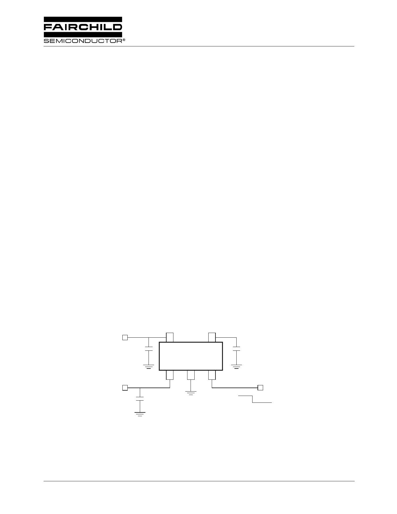
VOUT
COUT
VIN
CIN
5 SOT-23-5 4
ILC7083
123
CNOISE
ON
OFF
REV. 1.0.9 1/28/03
1 page 
ILC7083/ILC7084
Operation
The ILC7083/ILC7084 LDO design is based on an advanced
circuit configuration for which patent protection has been
applied. Typically it is very difficult to drive a capacitive out-
put with an amplifier. The output capacitance produces a
pole in the feedback path, which upsets the carefully tailored
dominant pole of the internal amplifier. Traditionally the
pole of the output capacitor has been “eliminated” by reduc-
ing the output impedance of the regulator such that the pole
of the output capacitor is moved well beyond the gain band-
width product of the regulator. In practice, this is difficult to
do and still maintain high frequency operation. Typically the
output impedance of the regulator is not simply resistive,
such that the reactive output impedance interacts with the
reactive impedance of the load resistance and capacitance.
In addition, it is necessary to place the dominant pole of
the circuit at a sufficiently low frequency such that the gain
of the regulator has fallen below unity before any of the
complex interactions between the output and the load occur.
The ILC7083/ILC7084 does not try to eliminate the output
pole, but incorporates it into the stability scheme. The load
and output capacitor forms a pole, which rolls off the gain of
the regulator below unity. In order to do this the output
impedance of the regulator must be high, looking like a
current source. The output stage of the regulator becomes a
transconductance amplifier, which converts a voltage to a
current with a substantial output impedance. The circuit
which drives the transconductance amplifier is the error
amplifier, which compares the regulator output to the band
gap reference and produces an error voltage as the input to
the transconductance amplifier. The error amplifier has a
dominant pole at low frequency and a “zero” which cancels
out the effects of the pole. The zero allows the regulator
to have gain out to the frequency where the output pole
continues to reduce the gain to unity. The configuration of
the poles and zero are shown in Figure 1. Instead of power-
ing the critical circuits from the unregulated input voltage,
the CMOS RF LDO powers the internal circuits such as the
bandgap, the error amplifier and most of the transconduc-
tance amplifier from the boot strapped regulated output
voltage of the regulator. This technique offers extremely high
ripple rejection and excellent line transient response.
DOMINANT POLE
85 dB
COMPENSATING
ZERO
UNITY GAIN
OUTPUT POLE
FREQUENCY
Figure 1. ILC7083/ILC7084 RF LDO Frequency Response
A block diagram of the regulator circuit used in the ILC7083
is shown in Figure 2, which shows the input-to-output isola-
tion and the cascaded sequence of amplifiers that implement
the pole-zero scheme outlined above.
The ILC7083/ILC7084 is designed in a CMOS process with
some minor additions, which allow the circuit to be used at
input voltages up to 13V. The resulting circuit exceeds the
frequency response of traditional bipolar circuits. The
ILC7083/ILC7084 is very tolerant of output load conditions
with the inclusion of both short circuit and thermal overload
protection. The device has a very low dropout voltage,
typically a linear response of 1mV per milliamp of load
current, and none of the quasi-saturation characteristics of a
bipolar output devices. All the good features of the frequency
response and regulation are valid right to the point where the
regulator goes out of regulation in a 4 millivolt transition
region. Because there is no base drive, the regulator is
capable of providing high current surges while remaining in
regulation. This is shown in the high peak current of 500mA
which allows for the ILC7083/ILC7084 to be used in
systems that require short burst mode operation.
REV. 1.0.9 1/28/03
5
5 Page 
ILC7083/ILC7084
Typical Performance Characteristics ILC7083/ILC7084
Unless otherwise specified: TA = 25°C, VIN = VOUT(NOM) + 1V, ON/OFF pin tied to VIN
3.015
3.01
3.005
3
Output Voltage vs Temperature
VOUT = 3.0V
COUT = 1µF (Ceramic)
Dropout Characteristics
3.4
VOUT = 3.3V
COUT = 1µF (Ceramic)
3.3 IOUT = 0mA
IOUT = 10mA
IOUT = 50mA
3.2
2.995
2.99
2.985
-50
0 50 100
Temperature (°C)
150
Dropout Voltage vs Temperature
250
VOUT = 3.0V
200
IOUT = 150mA
150 IOUT = 100mA
3.1 IOUT = 100mA
IOUT = 150mA
3
3 3.2 3.4 3.6
VIN (V)
Dropout Voltage vs IOUT
250
VOUT = 3.0V
200
TA = 85°C
TA = 25°C
150
100
IOUT = 50mA
50
0
–40
IOUT = 0mA
25
85
Temperature (°C)
100
50
0
0
TA = –40°C
50 100
Output Current (mA)
150
Ground Current vs Input Voltage
150
VOUT = 3.0 V
COUT = 1µF (Ceramic)
IOUT = 10mA
125 IOUT = 150mA IOUT = 50mA
IOUT = 0mA
100
IOUT = 100mA
75
50
2
4
6
8 10 12
14
VIN (V)
6
5
4
3.01
3.00
2.99
2.98
Line Transient Response
VIN: tr/tf < 1 µs
VOUT = 3.0V
COUT = 2.2 µF (Ceramic)
IOUT = 100 mA
5µs/div
REV. 1.0.9 1/28/03
11
11 Page | ||
| Páginas | Total 16 Páginas | |
| PDF Descargar | [ Datasheet ILC7084.PDF ] | |
Hoja de datos destacado
| Número de pieza | Descripción | Fabricantes |
| ILC708 | (ILC705 - ILC708) MP SUPERVISORY CIRCUIT | Impala Linear Corporation |
| ILC7080 | 50/100M SOT-23 CMOS RF LDO REGULATORS | Impala Linear Corporation |
| ILC7080 | 50/100mA SOT-23 CMOS RF LDO Regulators | Fairchild Semiconductor |
| ILC7080AIM5 | 50/100mA SOT-23 CMOS RF LDO Regulators | Fairchild Semiconductor |
| Número de pieza | Descripción | Fabricantes |
| SLA6805M | High Voltage 3 phase Motor Driver IC. |
Sanken |
| SDC1742 | 12- and 14-Bit Hybrid Synchro / Resolver-to-Digital Converters. |
Analog Devices |
|
DataSheet.es es una pagina web que funciona como un repositorio de manuales o hoja de datos de muchos de los productos más populares, |
| DataSheet.es | 2020 | Privacy Policy | Contacto | Buscar |