|
|
PDF 12C672 Data sheet ( Hoja de datos )
| Número de pieza | 12C672 | |
| Descripción | EPROM Memory Programming Specification | |
| Fabricantes | Microchip Technology | |
| Logotipo |  |
|
Hay una vista previa y un enlace de descarga de 12C672 (archivo pdf) en la parte inferior de esta página. Total 14 Páginas | ||
|
No Preview Available !
PIC12C67X AND PIC12CE67X
EPROM Memory Programming Specification
This document includes the programming
specifications for the following devices:
• PIC12C671
• PIC12C672
• PIC12CE673
• PIC12CE674
1.0 PROGRAMMING THE
PIC12C67X AND PIC12CE67X
The PIC12C67X and PIC12CE67X can be pro-
grammed using a serial method. In serial mode the
PIC12C67X and PIC12CE67X can be programmed
while in the users system. This allows for increased
design flexibility.
1.1 Hardware Requirements
The PIC12C67X and PIC12CE67X requires two pro-
grammable power supplies, one for VDD (2.0V to 6.0V
recommended) and one for VPP (12V to 14V). Both
supplies should have a minimum resolution of 0.25V.
1.2 Programming Mode
The programming mode for the PIC12C67X and
PIC12CE67X allows programming of user program
memory, special locations used for ID, and the configu-
ration word for the PIC12C67X and PIC12CE67X.
Pin Diagram:
PDIP
VDD
GP5/OSC1/CLKIN
GP4/OSC2/AN3/
CLKOUT
GP3/MCLR/VPP
1
2
3
4
8 VSS
7 GP0/AN0
6 GP1/AN1/VREF
5 GP2/T0CKI/
AN2/INT
PIN DESCRIPTIONS (DURING PROGRAMMING): PIC12C671/672 and PIC12CE673/674
Pin Name
Pin Name
GP1
CLOCK
GP0
DATA
GP3/MCLR/VPP
VPP
VDD
VDD
VSS
VSS
Legend: I = Input, O = Output, P = Power
During Programming
Pin Type
Pin Description
I Clock input
I/O Data input/output
P Programming Power
P Power Supply
P Ground
© 1998 Microchip Technology Inc.
DS40175A-page 1
1 page 
EPROM Memory Programming Specification
FIGURE 1-1: PROGRAM FLOW CHART - PIC12C67X AND PIC12CE67X PROGRAM MEMORY
Start
Set VPP = VIHH1
Set VDD = VDDP•
N=0
Program Cycle
No
N > 25
Yes Report Programming
Failure
Increment Address
Command
Read Data
Command
Data Correct?
Yes
N=N+1
N = # of Program Cycles
No
Apply 3N Additional
Program Cycles
No
All Locations Done?
Yes
Verify all Locations
@ VDD MIN.•
VPP = VIHH2
No
Data Correct?
Yes
Verify all Locations
@ VDD MAX.
VPP = VIHH2
Report Verify
@ VDD MIN. Error
Data Correct?
Yes
No Report Verify
@ VDD MAX Error
Done
• VDDP = VDD range for programming (typically 4.75V - 5.25V).
VDD MIN. = Minimum VDD for device operation.
VDD MAX. = Maximum VDD for device operation.
Program Cycle
Load Data
Command
Begin Programming
Command
Wait 100 µs
End Programming
Command
© 1998 Microchip Technology Inc.
DS40175A-page 5
5 Page 
EPROM Memory Programming Specification
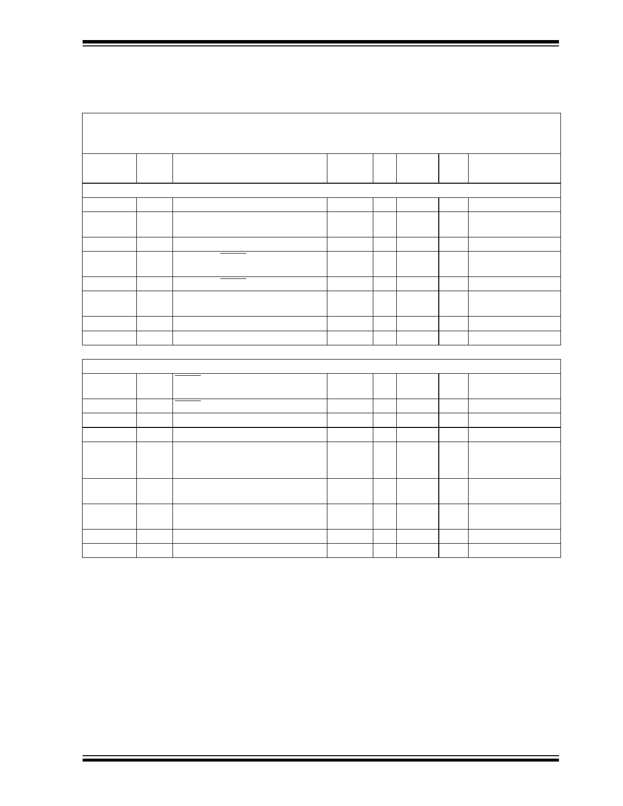
4.0 PROGRAM/VERIFY MODE ELECTRICAL CHARACTERISTICS
TABLE 4-1: AC/DC CHARACTERISTICS
TIMING REQUIREMENTS FOR PROGRAM/VERIFY TEST MODE
Standard Operating Conditions
Operating Temperature: +10°C ≤ TA ≤ +40°C, unless otherwise stated, (25°C is recommended)
Operating Voltage:
4.5V ≤ VDD ≤ 5.5V, unless otherwise stated.
Parameter
No.
Sym.
Characteristic
Min. Typ. Max. Units
Conditions
General
PD1
PD2
PD3
PD4
PD5
PD6
PD9
PD8
VDDP Supply voltage during programming
IDDP Supply current (from VDD)
during programming
VDDV Supply voltage during verify
VIHH1 Voltage on MCLR/VPP during
programming
VIHH2 Voltage on MCLR/VPP during verify
IPP Programming supply current (from
VPP)
VIH1 (GP0, GP1) input high level
VIL1 (GP0, GP1) input low level
4.75 5.0 5.25
20
VDDmin
12.75
VDDmax
13.25
VDD + 4.0
13.5
50
0.8 VDD
0.2 VDD
V
mA
V Note 1
V Note 2
mA
V Schmitt Trigger input
V Schmitt Trigger input
Serial Program Verify
P1 TR MCLR/VPP rise time (VSS to VIHH)
for test mode entry
8.0
P2 Tf MCLR Fall time
8.0
P3 Tset1 Data in setup time before clock ↓
100
P4 Thld1 Data in hold time after clock ↓
100
P5 Tdly1 Data input not driven to next clock
1.0
input (delay required between com-
mand/data or command/command)
P6
Tdly2 Delay between clock ↓ to clock ↑ of
1.0
next command or data
P7 Tdly3 Clock ↑ to data out valid
(during read data)
200
P8 Thld0 Hold time after VDD↑
2
P9 TPPDP Hold time after VPP↑
5
Note 1: Program must be verified at the minimum and maximum VDD limits for the part.
Note 2: VIHH must be greater than VDD + 4.5V to stay in programming/verify mode.
µs
µs
ns
ns
µs
µs
ns
µs
µs
© 1998 Microchip Technology Inc.
DS40175A-page 11
11 Page | ||
| Páginas | Total 14 Páginas | |
| PDF Descargar | [ Datasheet 12C672.PDF ] | |
Hoja de datos destacado
| Número de pieza | Descripción | Fabricantes |
| 12C671 | EPROM Memory Programming Specification | Microchip Technology |
| 12C671 | EPROM Memory Programming Specification | Microchip Technology |
| 12C672 | EPROM Memory Programming Specification | Microchip Technology |
| 12C672 | EPROM Memory Programming Specification | Microchip Technology |
| Número de pieza | Descripción | Fabricantes |
| SLA6805M | High Voltage 3 phase Motor Driver IC. |
Sanken |
| SDC1742 | 12- and 14-Bit Hybrid Synchro / Resolver-to-Digital Converters. |
Analog Devices |
|
DataSheet.es es una pagina web que funciona como un repositorio de manuales o hoja de datos de muchos de los productos más populares, |
| DataSheet.es | 2020 | Privacy Policy | Contacto | Buscar |
