|
|
PDF IDT70V639S Data sheet ( Hoja de datos )
| Número de pieza | IDT70V639S | |
| Descripción | HIGH-SPEED 3.3V 128K x 18 ASYNCHRONOUS DUAL-PORT STATIC RAM | |
| Fabricantes | Integrated Device Technology | |
| Logotipo |  |
|
Hay una vista previa y un enlace de descarga de IDT70V639S (archivo pdf) en la parte inferior de esta página. Total 23 Páginas | ||
|
No Preview Available !
HIGH-SPEED 3.3V 128K x 18
ASYNCHRONOUS DUAL-PORT
STATIC RAM
PRELIMINARY
IDT70V639S
Features
x True Dual-Port memory cells which allow simultaneous
access of the same memory location
x High-speed access
– Commercial: 10/12/15ns (max.)
– Industrial: 12/15ns (max.)
x Dual chip enables allow for depth expansion without
external logic
x IDT70V639 easily expands data bus width to 36 bits or
more using the Master/Slave select when cascading more
than one device
x M/S = VIH for BUSY output flag on Master,
M/S = VIL for BUSY input on Slave
x Busy and Interrupt Flags
x On-chip port arbitration logic
x Full on-chip hardware support of semaphore signaling
between ports
Functional Block Diagram
UBL
LBL
R/WL
CE0 L
CE1L
x Fully asynchronous operation from either port
x Separate byte controls for multiplexed bus and bus
matching compatibility
x Supports JTAG features compliant to IEEE 1149.1
– Due to limited pin count, JTAG is not supported on the
128-pin TQFP package.
x LVTTL-compatible, single 3.3V (±150mV) power supply for
core
x LVTTL-compatible, selectable 3.3V (±150mV)/2.5V (±100mV)
power supply for I/Os and control signals on each port
x Available in a 128-pin Thin Quad Flatpack, 208-ball fine
pitch Ball Grid Array, and 256-ball Ball Grid Array
x Industrial temperature range (–40°C to +85°C) is available
for selected speeds
BB
EE
01
LL
BB
EE
10
RR
UBR
LBR
R/WR
CE0R
CE1R
OEL
I/O0L- I/O17L
Dout0-8_L
Dout9-17_L
Dout0-8_R
Dout9-17_R
128K x 18
MEMORY
ARRAY
Din_L
Din_R
OER
I/O0R - I/O17R
A16L
A0L
Address
Decoder
ADDR_L
ADDR_R
Address
Decoder
A16 R
A0R
BUSYL
SEML
INTL
CE0L
CE1L
OEL
R/WL
ARB ITR ATIO N
I NT ERRU PT
SEMAPHORE
LOGIC
M/S
TDI
TDO
JTAG
NOTES:
1. BUSY is an input as a Slave (M/S=VIL) and an output when it is a Master (M/S=VIH).
2. BUSY and INT are non-tri-state totem-pole outputs (push-pull).
©2001 Integrated Device Technology, Inc.
1
OER
R/ WR
CE0 R
CE1R
TMS
TCK
TRST
BUSYR
SEM R
INTR
5621 drw 01
JUNE 2001
DSC-5621/3
1 page 
IDT70V639S
High-Speed 3.3V 128K x 18 Asynchronous Dual-Port Static RAM
Preliminary
Industrial and Commercial Temperature Ranges
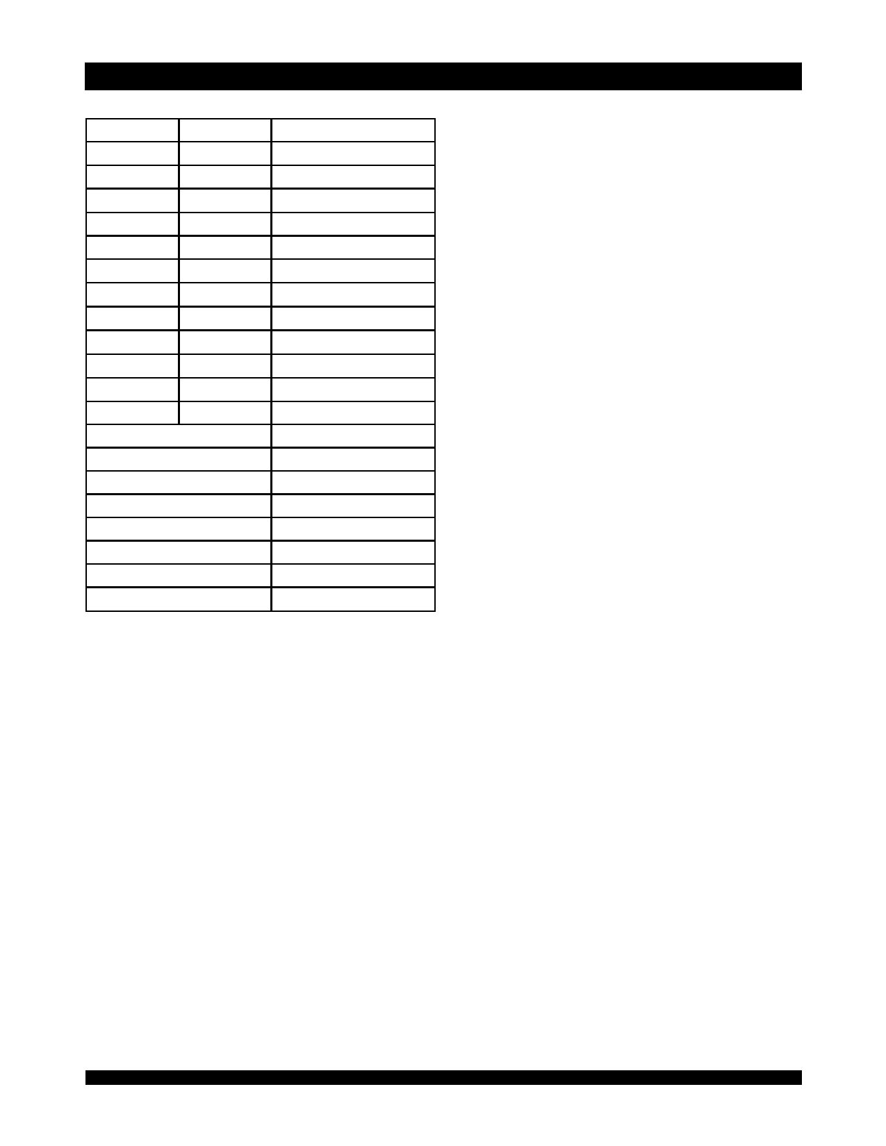
Pin Names
Left Port
Right Port
Names
CE0L, CE1L
R/WL
CE0R, CE1R
R/WR
Chip Enables
Read/Write Enable
OEL OER Output Enable
A0L - A16L
A0R - A16R
Address
I/O0L - I/O17L
I/O0R - I/O17R
Data Input/Output
SEML
SEMR
Semaphore Enable
INTL INTR Interrupt Flag
BUSYL
BUSYR
Busy Flag
UBL UBR Upper Byte Select
LBL
VDDQL
OPTL
LBR
VDDQR
OPTR
M/S
Lower Byte Select
Power (I/O Bus) (3.3V or 2.5V)(1)
Option for selecting VDDQX(1,2)
Master or Slave Select
VDD Power (3.3V)(1)
VSS
TDI
TDO
TCK
TMS
TRST
Ground (0V)
Test Data Input
Test Data Output
Test Logic Clock (10MHz)
Test Mode Select
Reset (Initialize TAP Controller)
5621 tbl 01
NOTES:
1. VDD, OPTX, and VDDQX must be set to appropriate operating levels prior to
applying inputs on I/OX.
2. OPTX selects the operating voltage levels for the I/Os and controls on that port.
If OPTX is set to VIH (3.3V), then that port's I/Os and controls will operate at 3.3V
levels and VDDQX must be supplied at 3.3V. If OPTX is set to VIL (0V), then that
port's I/Os and controls will operate at 2.5V levels and VDDQX must be supplied
at 2.5V. The OPT pins are independent of one another—both ports can operate
at 3.3V levels, both can operate at 2.5V levels, or either can operate at 3.3V
with the other at 2.5V.
5
5 Page 
IDT70V639S
High-Speed 3.3V 128K x 18 Asynchronous Dual-Port Static RAM
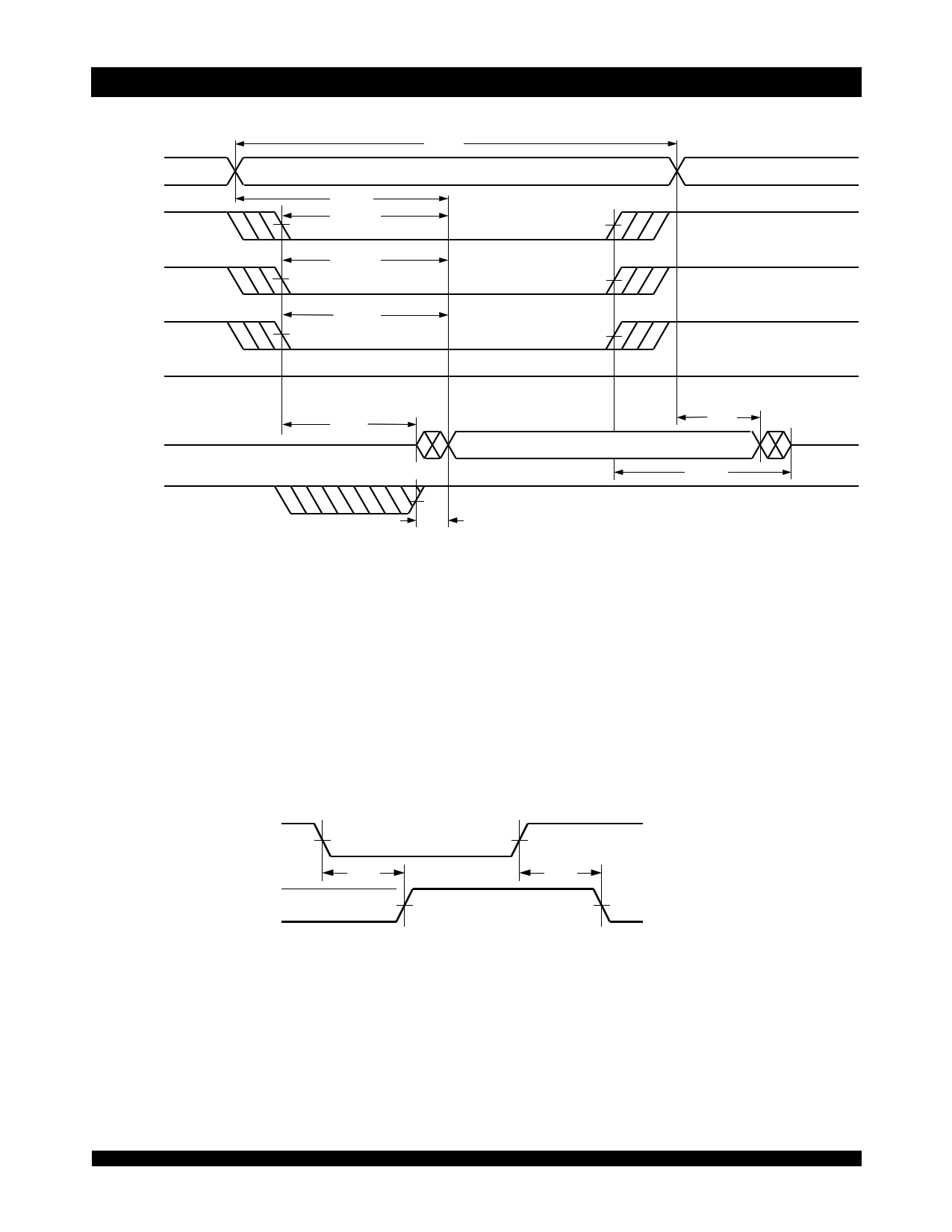
Waveform of Read Cycles(5)
tRC
ADDR
CE(6)
tAA (4)
tACE (4)
tAOE (4)
OE
UB, LB
tABE (4)
Preliminary
Industrial and Commercial Temperature Ranges
R/W
DATAOUT
tLZ (1)
(4)
VALID DATA
tOH
BUSYOUT
tBDD (3,4)
tHZ (2)
5621 drw 06
NOTES:
1. Timing depends on which signal is asserted last, OE, CE, LB or UB.
2. Timing depends on which signal is de-asserted first CE, OE, LB or UB.
3. tBDD delay is required only in cases where the opposite port is completing a write operation to the same address location. For simultaneous read operations BUSY
has no relation to valid output data.
4. Start of valid data depends on which timing becomes effective last tAOE, tACE, tAA or tBDD.
5. SEM = VIH.
Timing of Power-Up Power-Down
CE
tPU
ICC
50%
ISB
tPD
50%
.
5621 drw 07
11
11 Page | ||
| Páginas | Total 23 Páginas | |
| PDF Descargar | [ Datasheet IDT70V639S.PDF ] | |
Hoja de datos destacado
| Número de pieza | Descripción | Fabricantes |
| IDT70V639S | HIGH-SPEED 3.3V 128K x 18 ASYNCHRONOUS DUAL-PORT STATIC RAM | Integrated Device Technology |
| Número de pieza | Descripción | Fabricantes |
| SLA6805M | High Voltage 3 phase Motor Driver IC. |
Sanken |
| SDC1742 | 12- and 14-Bit Hybrid Synchro / Resolver-to-Digital Converters. |
Analog Devices |
|
DataSheet.es es una pagina web que funciona como un repositorio de manuales o hoja de datos de muchos de los productos más populares, |
| DataSheet.es | 2020 | Privacy Policy | Contacto | Buscar |
