|
|
|
PDF IDT70V27 Data sheet ( Hoja de datos )
| Número de pieza | IDT70V27 | |
| Descripción | HIGH-SPEED 3.3V 32K x 16 DUAL-PORT STATIC RAM | |
| Fabricantes | Integrated Device Technology | |
| Logotipo | ||
Hay una vista previa y un enlace de descarga de IDT70V27 (archivo pdf) en la parte inferior de esta página. Total 22 Páginas | ||
|
No Preview Available !
HIGH-SPEED 3.3V
32K x 16 DUAL-PORT
STATIC RAM
IDT70V27S/L
Features:
x True Dual-Ported memory cells which allow simultaneous
access of the same memory location
x High-speed access
– Industrial: 35ns (max.)
– Commercial: 15/20/25/35/55ns (max.)
x Low-power operation
– IDT70V27S
Active: 500mW (typ.)
Standby: 3.3mW (typ.)
– IDT70V27L
Active: 500mW (typ.)
Standby: 660µW (typ.)
x Separate upper-byte and lower-byte control for bus
matching capability
x Dual chip enables allow for depth expansion without
external logic
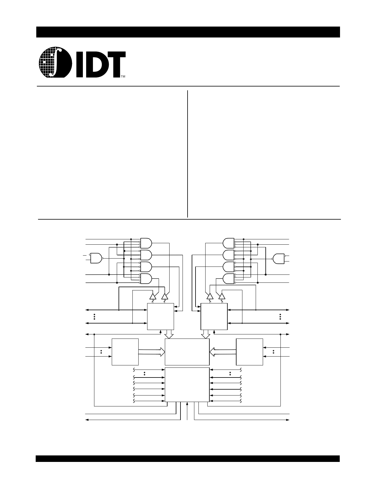
Functional Block Diagram
R/WL
UBL
CE0L
CE1L
OEL
LBL
x IDT70V27 easily expands data bus width to 32 bits or more
using the Master/Slave select when cascading more than
one device
x M/S = VIH for BUSY output flag on Master,
M/S = VIL for BUSY input on Slave
x Busy and Interrupt Flags
x On-chip port arbitration logic
x Full on-chip hardware support of semaphore signaling
between ports
x Fully asynchronous operation from either port
x LVTTL-compatible, single 3.3V (±0.3V) power supply
x Available in 100-pin Thin Quad Flatpack (TQFP), 108-pin
Ceramic Pin Grid Array (PGA), and 144-pin Fine Pitch BGA
(fpBGA)
x Industrial temperature range (-40°C to +85°C) is available
for selected speeds
R/WR
UBR
CE0R
CE1R
OER
LBR
I/O8-15L
I/O0-7L
BUSYL (1,2)
I/O
Control
I/O
Control
A14L
A0L
Address
Decoder
A14L
A0L
CE0L
CE1L
OEL
R/WL
32Kx16
MEMORY
ARRAY
70V27
ARBITRATION
INTERRUPT
SEMAPHORE
LOGIC
SEM L
NOTES:
INT
(2)
L
M/S (2)
1) BUSY is an input as a Slave (M/S=VIL) and an output as a Master (M/S=VIH).
2) BUSY and INT are non-tri-state totem-pole outputs (push-pull).
©2000 Integrated Device Technology, Inc.
6.011
Address
Decoder
A14R
A0R
CE0R
CE1R
OER
R/WR
I/O8-15R
I/O0-7R
BUSYR(1,2)
A14R
A0R
SEMR
INTR(2)
3603 drw 01
JANUARY 2001
DSC 3603/7
1 page 
IDT 70V27S/L
High-Speed 3.3V 32K x 16 Dual-Port Static RAM
Truth Table I Chip Enable(1,2,3)
Commercial and Industrial Temperature Range
CE CE0
CE1
Mode
VIL VIH Port Selected (TTL Active)
L
< 0.2V
>VCC -0.2V
Port Selected (CMOS Active)
VIH X Port Deselected (TTL Inactive)
X
H >VCC -0.2V
VIL Port Deselected (TTL Inactive)
X Port Deselected (CMOS Inactive)
X
<0.2V
Port Deselected (CMOS Inactive)
NOTES:
1. Chip Enable references are shown above with the actual CE0 and CE1 levels, CE is a reference only.
2. Port "A" and "B" references are located where CE is used.
3. "H" = VIH and "L" = VIL
3603 tbl 02
Truth Table II Non-Contention Read/Write Control
Inputs(1)
Outputs
CE(2)
R/W
OE
UB
LB SEM I/O8-15 I/O0-7
Mode
H
X
X
X
X
H
High-Z
High-Z Deselected: Power-Down
X
X
X
H
H
H
High-Z
High-Z Both Bytes Deselected
L
L
X
L
H
H
DATAIN
High-Z Write to Upper Byte Only
L
L
X
H
L
H
High-Z
DATAIN Write to Lower Byte Only
L
L
X
L
L
H
DATAIN
DATAIN Write to Both Bytes
L H L L H H DATAOUT High-Z Read Upper Byte Only
L H L H L H High-Z DATAOUT Read Lower Byte Only
L H L L L H DATAOUT DATAOUT Read Both Bytes
X
X
H
X
X
X
High-Z
High-Z Outputs Disabled
NOTES:
1. A0L — A14L ≠ A0R — A14R.
2. Refer to Chip Enable Truth Table.
3603 tbl 03
Truth Table III Semaphore Read/Write Control
Inputs(1)
Outputs
CE(2)
R/W
OE
UB
LB SEM I/O8-15 I/O0-7
Mode
H H L X X L DATAOUT DATAOUT Read Data in Semaphore Flag
X H L H H L DATAOUT DATAOUT Read Data in Semaphore Flag
H
↑
X
X
X
L
DATAIN
DATAIN Write I/O0 into Semaphore Flag
X
↑
X
H
H
L
DATAIN
DATAIN Write I/O0 into Semaphore Flag
L X X L X L ______ ______ Not Allowed
L X X X L L ______ ______ Not Allowed
NOTES:
1. There are eight semaphore flags written to I/O0 and read from all the I/Os (I/O0-I/O15). These eight semaphore flags are addressed by A0-A2.
2. Refer to Chip Enable Truth Table.
3603 tbl 04
5
5 Page 
IDT 70V27S/L
High-Speed 3.3V 32K x 16 Dual-Port Static RAM
Commercial and Industrial Temperature Range
AC Electrical Characteristics Over the
Operating Temperature and Supply Voltage(5,6)
70V27X15
Com'l Only
70V27X20
Com'l Only
70V27X25
Com'l Only
Symbol
Parameter
Min. Max. Min. Max. Min. Max. Unit
WRITE CYCLE
tWC Write Cycle Time
15 ____ 20 ____ 25 ____ ns
tEW Chip Enable to End-of-Write(3)
12 ____ 15 ____ 20 ____ ns
tAW Address Valid to End-of-Write
12 ____ 15 ____ 20 ____ ns
tAS Address Set-up Time(3)
0 ____ 0 ____ 0 ____ ns
tWP Write Pulse Width
12 ____ 15 ____ 20 ____ ns
tWR Write Recovery Time
0 ____ 0 ____ 0 ____ ns
tDW Data Valid to End-of-Write
10 ____
15 ____
15 ____
ns
tHZ Output High-Z Time (1,2)
____ 10 ____ 10 ____ 15 ns
tDH Data Hold Time (4)
0 ____ 0 ____ 0 ____ ns
tWZ Write Enable to Output in High-Z (1,2)
____ 10 ____ 10 ____ 15 ns
tOW Output Active from End-of-Write (1,2,4)
0 ____ 0 ____ 0 ____ ns
tSWRD
tSPS
SEM Flag Write to Read Time
SEM Flag Contention Window
5 ____ 5 ____ 5 ____ ns
5 ____ 5 ____ 5 ____ ns
3603 tbl 13a
70V27X35
Com'l & Ind
70V27X55
Com'l Only
Symbol
Parameter
Min. Max. Min. Max. Unit
WRITE CYCLE
tWC Write Cycle Time
35 ____ 55 ____ ns
tEW Chip Enable to End-of-Write(3)
30 ____ 45 ____ ns
tAW Address Valid to End-of-Write
30 ____ 45 ____ ns
tAS Address Set-up Time(3)
0 ____ 0 ____ ns
tWP Write Pulse Width
25 ____ 40 ____ ns
tWR Write Recovery Time
0 ____ 0 ____ ns
tDW Data Valid to End-of-Write
20 ____ 30 ____ ns
tHZ Output High-Z Time (1,2)
____ 20 ____ 25 ns
tDH Data Hold Time (4)
0 ____ 0 ____ ns
tWZ Write Enable to Output in High-Z (1,2)
____ 20 ____ 25 ns
tOW Output Active from End-of-Write (1,2,4)
0 ____ 0 ____ ns
tSWRD
tSPS
SEM Flag Write to Read Time
SEM Flag Contention Window
5 ____ 5 ____ ns
5 ____ 5 ____ ns
NOTES:
3603 tbl 13b
1. Transition is measured 0mV from Low or High-impedance voltage with Output Test Load (Figure 2).
2. This parameter is guaranteed by device characterization, but is not production tested.
3. To access RAM CE= VIL and SEM = VIH. To access semaphore, CE = VIH and SEM = VIL. Either condition must be valid for the entire tEW time. Refer to Chip Enable
Truth Table.
4. The specification for tDH must be met by the device supplying write data to the RAM under all operating conditions. Although tDH and tOW values will vary over voltage
and temperature, the actual tDH will always be smaller than the actual tOW.
5. 'X' in part numbers indicates power rating (S or L).
6. Industrial temperature: for other speeds, packages and powers contact your sales office.
11
11 Page | ||
| Páginas | Total 22 Páginas | |
| PDF Descargar | [ Datasheet IDT70V27.PDF ] | |
Hoja de datos destacado
| Número de pieza | Descripción | Fabricantes |
| IDT70V24 | HIGH-SPEED 3.3V 4K x 16 DUAL-PORT STATIC RAM | Integrated Device Technology |
| IDT70V25 | HIGH-SPEED 3.3V 8K x 16 DUAL-PORT STATIC RAM | Integrated Device Technology |
| IDT70V26 | HIGH-SPEED 3.3V 16K x 16 DUAL-PORT STATIC RAM | Integrated Device Technology |
| IDT70V261L | HIGH-SPEED 3.3V 16K x 16 DUAL-PORT STATIC RAM | Integrated Device Technology |
| Número de pieza | Descripción | Fabricantes |
| SLA6805M | High Voltage 3 phase Motor Driver IC. |
Sanken |
| SDC1742 | 12- and 14-Bit Hybrid Synchro / Resolver-to-Digital Converters. |
Analog Devices |
|
DataSheet.es es una pagina web que funciona como un repositorio de manuales o hoja de datos de muchos de los productos más populares, |
| DataSheet.es | 2020 | Privacy Policy | Contacto | Buscar |