|
|
PDF IDT74FCT163646C Data sheet ( Hoja de datos )
| Número de pieza | IDT74FCT163646C | |
| Descripción | 3.3V CMOS 16-BIT BUS TRANSCEIVER/ REGISTERS | |
| Fabricantes | Integrated Device Technology | |
| Logotipo |  |
|
Hay una vista previa y un enlace de descarga de IDT74FCT163646C (archivo pdf) en la parte inferior de esta página. Total 9 Páginas | ||
|
No Preview Available !
Integrated Device Technology, Inc.
3.3V CMOS
16-BIT BUS TRANSCEIVER/
REGISTERS
IDT74FCT163646/A/C
FEATURES:
• 0.5 MICRON CMOS Technology
• Typical tSK(o) (Output Skew) < 250ps
• ESD > 2000V per MIL-STD-883, Method 3015;
> 200V using machine model (C = 200pF, R = 0)
• Packages include 25 mil pitch SSOP, 19.6 mil pitch
TSSOP and 15.7 mil pitch TVSOP
• Extended commercial range of -40°C to +85°C
• VCC = 3.3V ±0.3V, Normal Range or
VCC = 2.7 to 3.6V, Extended Range
• CMOS power levels (0.4µW typ. static)
• Rail-to-Rail output swing for increased noise margin
• Low Ground Bounce (0.3V typ.)
• Inputs (except I/O) can be driven by 3.3V or 5V
components
DESCRIPTION:
The FCT163646/A/C 16-bit registered transceivers are
built using advanced dual metal CMOS technology. These
high-speed, low-power devices are organized as two inde-
pendant 8-bit bus transceivers with 3-state D-type registers.
The control circuitry is organized for multiplexed transmission
of data between A bus and B bus either directly or from the
internal storage registers. Each 8-bit transceiver/register
features direction control (xDIR), over-riding Output Enable
control (xOE) and Select lines (xSAB and xSBA) to select
either real-time data or stored data. Separate clock inputs are
provided for A and B port registers. Data on the A or B data
bus, or both, can be stored in the internal registers by the
LOW-to-HIGH transitions at the appropriate clock pins. Flow-
through organization of signal pins simplifies layout. All inputs
are designed with hysteresis for improved noise margin.
The FCT163646/A/C have series current limiting resistors.
This offers low ground bounce, minimal undershoot, and
controlled output fall times-reducing the need for external
series terminating resistors.
FUNCTIONAL BLOCK DIAGRAM
1OE
1DIR
1CLKBA
1SBA
1CLKAB
1SAB
1A1 A REG
D
C
B REG
D
C
2OE
2DIR
2CLKBA
2SBA
2CLKAB
2SAB
1B1 2A1
A REG
D
C
B REG
D
C
2B1
TO 7 OTHER CHANNELS
2778 drw 01
TO 7 OTHER CHANNELS
2778 drw 02
The IDT logo is a registered trademark of Integrated Device Technology, Inc.
COMMERCIAL TEMPERATURE RANGES
©1996 Integrated Device Technology, Inc.
8.8
AUGUST 1996
DSC-2778/6
1
1 page 
IDT74FCT163646/A/C
3.3V 16-BIT BUS TRANSCEIVER/REGISTERS
COMMERCIAL TEMPERATURE RANGES
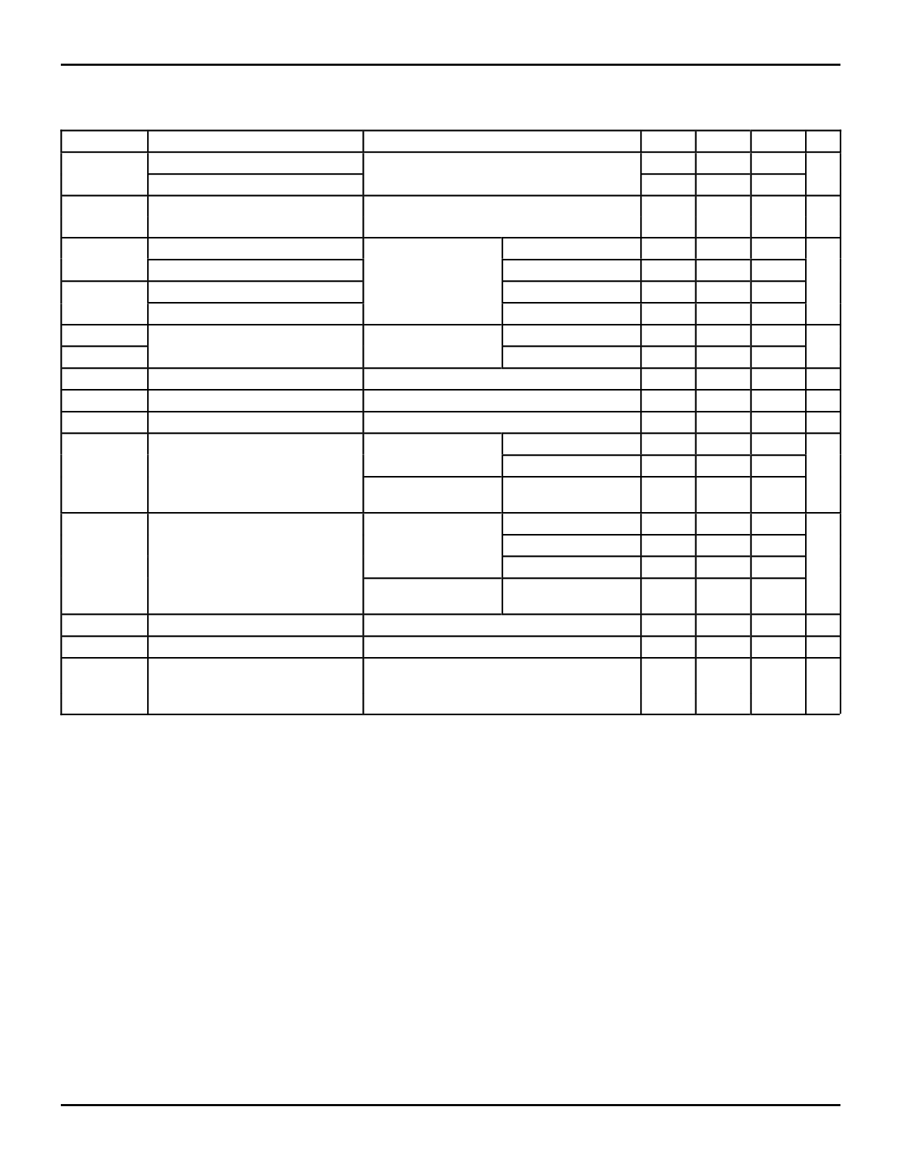
DC ELECTRICAL CHARACTERISTICS OVER OPERATING RANGE
Following Conditions Apply Unless Otherwise Specified:
Commercial: TA = –40°C to +85°C, VCC = 2.7V to 3.6V
Symbol
VIH
VIL
II H
II L
IOZH
IOZL
VIK
IODH
IODL
VOH
Parameter
Input HIGH Level (Input pins)
Input HIGH Level (I/O pins)
Input LOW Level
(Input and I/O pins)
Input HIGH Current (Input pins)
Input HIGH Current (I/O pins)
Input LOW Current (Input pins)
Input LOW Current (I/O pins)
High Impedance Output Current
(3-State Output pins)
Clamp Diode Voltage
Output HIGH Current
Output LOW Current
Output HIGH Voltage
Test Conditions(1)
Guaranteed Logic HIGH Level
Guaranteed Logic LOW Level
VCC = Max.
VI = 5.5V
VI = VCC
VI = GND
VI = GND
VCC = Max.
VO = VCC
VO = GND
VCC = Min., IIN = –18mA
VCC = 3.3V, VIN = VIH or VIL, VO = 1.5V(3)
VCC = 3.3V, VIN = VIH or VIL, VO = 1.5V(3)
VCC = Min.
IOH = –0.1mA
Min.
2.0
2.0
–0.5
Typ.(2) Max. Unit
— 5.5 V
— VCC+0.5
— 0.8 V
—
—
—
—
—
—
—
–36
50
VCC–0.2
—
—
—
—
—
—
–0.7
–60
90
—
±1
±1
±1
±1
±1
±1
–1.2
–110
200
—
µA
µA
V
mA
mA
V
VOL Output LOW Voltage
VIN = VIH or VIL
VCC = 3.0V
VIN = VIH or VIL
VCC = Min.
VIN = VIH or VIL
IOH = –3mA
IOH = –8mA
IOL = 0.1mA
IOL = 16mA
IOL = 24mA
2.4
2.4(5)
—
—
—
3.0
3.0
—
0.2
0.3
—
—
0.2
0.4
0.55
V
IOS Short Circuit Current(4)
VCC = 3.0V
IOL = 24mA
VIN = VIH or VIL
VCC = Max., VO = GND(3)
— 0.3 0.50
–60 –135 –240 mA
VH
ICCL
ICCH
ICCZ
Input Hysteresis
Quiescent Power Supply Current
VCC = Max.,
VIN = GND or VCC
—
— 150
— 0.1
NOTES:
1. For conditions shown as Max. or Min., use appropriate value specified under Electrical Characteristics for the applicable device type.
2. Typical values are at Vcc = 3.3V, +25°C ambient.
3. Not more than one output should be tested at one time. Duration of the test should not exceed one second.
4. This parameter is guaranteed but not tested.
5. VOH = VCC –0.6V at rated current.
— mV
10 µA
2778 lnk 05
8.8 5
5 Page | ||
| Páginas | Total 9 Páginas | |
| PDF Descargar | [ Datasheet IDT74FCT163646C.PDF ] | |
Hoja de datos destacado
| Número de pieza | Descripción | Fabricantes |
| IDT74FCT163646 | 3.3V CMOS 16-BIT BUS TRANSCEIVER/ REGISTERS | Integrated Device Technology |
| IDT74FCT163646A | 3.3V CMOS 16-BIT BUS TRANSCEIVER/ REGISTERS | Integrated Device Technology |
| IDT74FCT163646APA | 3.3V CMOS 16-BIT BUS TRANSCEIVER/ REGISTERS | Integrated Device Technology |
| IDT74FCT163646APF | 3.3V CMOS 16-BIT BUS TRANSCEIVER/ REGISTERS | Integrated Device Technology |
| Número de pieza | Descripción | Fabricantes |
| SLA6805M | High Voltage 3 phase Motor Driver IC. |
Sanken |
| SDC1742 | 12- and 14-Bit Hybrid Synchro / Resolver-to-Digital Converters. |
Analog Devices |
|
DataSheet.es es una pagina web que funciona como un repositorio de manuales o hoja de datos de muchos de los productos más populares, |
| DataSheet.es | 2020 | Privacy Policy | Contacto | Buscar |
