|
|
|
PDF IDT7208L25J Data sheet ( Hoja de datos )
| Número de pieza | IDT7208L25J | |
| Descripción | CMOS ASYNCHRONOUS FIFO 65/536 x 9 | |
| Fabricantes | Integrated Device Technology | |
| Logotipo | ||
Hay una vista previa y un enlace de descarga de IDT7208L25J (archivo pdf) en la parte inferior de esta página. Total 14 Páginas | ||
|
No Preview Available !
CMOS ASYNCHRONOUS FIFO
2,048 x 9, 4,096 x 9
8,192 x 9, 16,384 x 9
32,768 x 9 and 65,536 x 9
IDT7203
IDT7204
IDT7205
IDT7206
IDT7207
IDT7208
FEATURES:
• First-In/First-Out Dual-Port memory
• 2,048 x 9 organization (IDT7203)
• 4,096 x 9 organization (IDT7204)
• 8,192 x 9 organization (IDT7205)
• 16,384 x 9 organization (IDT7206)
• 32,768 x 9 organization (IDT7207)
• 65,636 x 9 organization (IDT7208)
• High-speed: 12ns access time
• Low power consumption
— Active: 660mW (max.)
— Power-down: 44mW (max.)
• Asynchronous and simultaneous read and write
• Fully expandable in both word depth and width
• 720x family is pin and functionally compatible from 256 x 9 to 64k x 9
• Status Flags: Empty, Half-Full, Full
• Retransmit capability
• High-performance CMOS technology
• Military product compliant to MIL-STD-883, Class B
• Standard Military Drawing for #5962-88669 (IDT7203), 5962-89567
(IDT7203), and 5962-89568 (IDT7204) are listed on this function
• Industrial temperature range (–40°C to +85°C) is available
(plastic packages only)
• Green parts available, see ordering information
DESCRIPTION:
The IDT7203/7204/7205/7206/7207/7208 are dual-port memory buffers
with internal pointers that load and empty data on a first-in/first-out basis. The
device uses Full and Empty flags to prevent data overflow and underflow and
expansion logic to allow for unlimited expansion capability in both word size and
depth.
Data is toggled in and out of the device through the use of the Write (W) and
Read (R) pins.
The device's 9-bit width provides a bit for a control or parity at the user’s
option. ItalsofeaturesaRetransmit(RT)capabilitythatallowsthereadpointer
to be reset to its initial position when RT is pulsed LOW. A Half-Full Flag is
available in the single device and width expansion modes.
These FIFOs are fabricated using high-speed CMOS technology. They
are designed for applications requiring asynchronous and simultaneous read/
writes in multiprocessing, rate buffering and other applications.
Military grade product is manufactured in compliance with MIL-STD-883,
Class B.
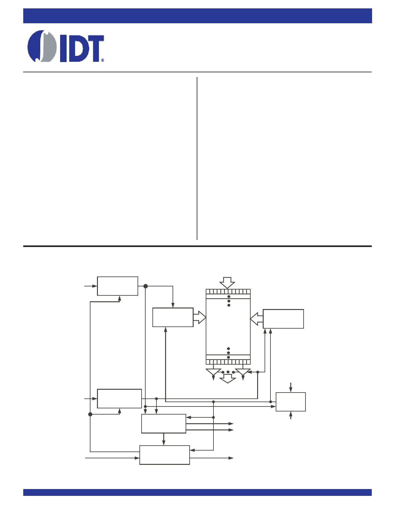
FUNCTIONAL BLOCK DIAGRAM
W
WRITE
CONTROL
DATA INPUTS
(D0 -D8)
WRITE
POINTER
RAM ARRAY
2,048 x 9
4,096 x 9
8,192 x 9
16,384 x 9
32,768 x 9
65,536 x 9
READ
POINTER
READ
R CONTROL
THREE-
STATE
BUFFERS
DATA OUTPUTS
(Q0-Q 8)
FLAG
LOGIC
EF
FF
EXPANSION
XI
LOGIC
XO/HF
IDT and the IDT logo are registered trademarks of Integrated Device Technology, Inc.
COMMERCIAL, MILITARY AND INDUSTRIAL TEMPERATURE RANGES
1
© 2012 Integrated Device Technology, Inc. All rights reserved. Product subject to change without notice.
RS
RESET
LOGIC
FL/RT
2661 drw01
JUNE 2012
DSC-2661/18
1 page 
IDT7203/7204/7205/7206/7207/7208 CMOS ASYNCHRONOUS FIFO
2,048 x 9, 4,096 x 9, 8,192 x 9, 16,384 x 9, 32,768 x 9 and 65,536 x 9
COMMERCIAL, INDUSTRIAL AND MILITARY
TEMPERATURERANGES
AC ELECTRICAL CHARACTERISTICS(1) (CONTINUED)
(Commercial: VCC = 5V ± 10%, TA = 0°C to +70°C; Industrial: VCC = 5V ± 10%, TA = –40°C to +85°C; Military: VCC = 5V ± 10%, TA = –55°C to +125°C)
Military
IDT7203L30
IDT7204L30
IDT7205L30
IDT7206L30
IDT7207L30
Commercial
IDT7203L35
IDT7204L35
IDT7205L35
IDT7206L35
IDT7207L35
IDT7208L35
Military
IDT7203L40
Commercial
IDT7203L50
IDT7204L50
IDT7205L50
IDT7206L50
IDT7207L50
Symbol
fS
tRC
tA
tRR
tRPW
tRLZ
tWLZ
tDV
tRHZ
tWC
tWPW
tWR
tDS
tDH
tRSC
tRS
tRSS
tRTR
tRTC
tRT
tRTS
tRTR
tEFL
tHFH, tFFH
tRTF
tREF
tRFF
tRPE
tWEF
tWFF
tWHF
tRHF
tWPF
tXOL
tXOH
tXI
tXIR
tXIS
Parameters
Shift Frequency
Read Cycle Time
Access Time
Read Recovery Time
Read Pulse Width(2)
Read LOW to Data Bus LOW(3)
Write HIGH to Data Bus Low-Z(3,4)
Data Valid from Read HIGH
Read HIGH to Data Bus High-Z(3)
Write Cycle Time
Write Pulse Width(2)
Write Recovery Time
Data Set-up Time
Data Hold Time
Reset Cycle Time
Reset Pulse Width(2)
Reset Set-up Time(3)
Reset Recovery Time
Retransmit Cycle Time
Retransmit Pulse Width(2)
Retransmit Set-up Time(3)
Retransmit Recovery Time
Reset to EF LOW
Reset to HF and FF HIGH
Retransmit LOW to Flags Valid
Read LOW to EF LOW
Read HIGH to FF HIGH
Read Pulse Width after EF HIGH
Write HIGH to EF HIGH
Write LOW to FF LOW
Write LOW to HF Flag LOW
Read HIGH to HF Flag HIGH
Write Pulse Width after FF HIGH
Read/Write LOW to XO LOW
Read/Write HIGH to XO HIGH
XI Pulse Width(2)
XI Recovery Time
XISet-up Time
Min. Max.
— 25
40 —
— 30
10 —
30 —
5—
5—
5—
— 20
40 —
30 —
10 —
18 —
0—
40 —
30 —
30 —
10 —
40 —
30 —
30 —
10 —
— 40
— 40
— 40
— 30
— 30
30 —
— 30
— 30
— 40
— 40
30 —
— 30
— 30
30 —
10 —
10 —
Min. Max. Min. Max. Min. Max. Unit
— 22.22
—
20
—
15 MHz
45 — 50 — 65 — ns
— 35 — 40 — 50 ns
10 — 10 — 15 — ns
35 — 40 — 50 — ns
5 — 5 — 10 — ns
10 — 10 — 15 — ns
5 — 5 — 5 — ns
— 20 — 25 — 30 ns
45 — 50 — 65 — ns
35 — 40 — 50 — ns
10 — 10 — 15 — ns
18 — 20 — 30 — ns
0 — 0 — 5 — ns
45 — 50 — 65 — ns
35 — 40 — 50 — ns
35 — 40 — 50 — ns
10 — 10 — 15 — ns
45 — 50 — 65 — ns
35 — 40 — 50 — ns
35 — 40 — 50 — ns
10 — 10 — 15 — ns
— 45 — 50 — 65 ns
— 45 — 50 — 65 ns
— 45 — 50 — 65 ns
— 30 — 35 — 45 ns
— 30 — 35 — 45 ns
35 — 40 — 50 — ns
— 30 — 35 — 45 ns
— 30 — 35 — 45 ns
— 45 — 50 — 65 ns
— 45 — 50 — 65 ns
35 — 40 — 50 — ns
— 35 — 40 — 50 ns
— 35 — 40 — 50 ns
35 — 40 — 50 — ns
10 — 10 — 10 — ns
15 — 15 — 15 — ns
NOTES:
1. Timings referenced as in AC Test Conditions.
2. Pulse widths less than minimum are not allowed.
3. Values guaranteed by design, not currently tested.
4. Only applies to read data flow-through mode.
5
5 Page 
IDT7203/7204/7205/7206/7207/7208 CMOS ASYNCHRONOUS FIFO
2,048 x 9, 4,096 x 9, 8,192 x 9, 16,384 x 9, 32,768 x 9 and 65,536 x 9
COMMERCIAL, INDUSTRIAL AND MILITARY
TEMPERATURERANGES
TRUTH TABLES
TABLE 1 – RESET AND RETRANSMIT
SINGLE DEVICE CONFIGURATION/WIDTH EXPANSION MODE
Inputs
Internal Status
Mode
RS FL/RT XI
Read Pointer
Write Pointer
Reset
Retransmit
Read/Write
0 X 0 LocationZero
LocationZero
1 0 0 LocationZero Unchanged
1 1 0 Increment(1)
Increment(1)
NOTE:
1. Pointer will Increment if flag is HIGH.
TABLE 2 – RESET AND FIRST LOAD
DEPTH EXPANSION/COMPOUND EXPANSION MODE
Inputs
Internal Status
Mode
RS FL/RT XI Read Pointer
Write Pointer
Reset First Device
0 0 (1) LocationZero
LocationZero
Reset All Other Devices
Read/Write
0 1 (1) LocationZero
1 X (1)
X
LocationZero
X
Outputs
EF FF
01
XX
XX
HF
1
X
X
Outputs
EF FF
01
01
XX
NOTES:
1. XI is connected to XO of previous device. See Figure 14.
2. RS = Reset Input, FL/RT = First Load/Retransmit, EF = Empty Flag Output, FF = Full Flag Output, XI = Expansion Input, HF = Half-Full Flag Output
W
D9
FULL
RS
FF
9
FF
9
FF
9
XO
IDT
7203
7204
7205
7206
7207
7208
XI
XO
IDT
7203
7204
7205
7206
7207
7208
XI
XO
IDT
7203
7204
7205
7206
7207
7208
XI
EF
FL
EF
FL
EF
FL
9
R
Q
VCC
EMPTY
2661 drw16
Figure 14. Block Diagram of 6,144 x 9, 12,288 x 9, 24,576 x 9, 49,152 x 9, 98,304 x 9, 196,608 x 9 FIFO Memory (Depth Expansion)
11
11 Page | ||
| Páginas | Total 14 Páginas | |
| PDF Descargar | [ Datasheet IDT7208L25J.PDF ] | |
Hoja de datos destacado
| Número de pieza | Descripción | Fabricantes |
| IDT7208L25J | CMOS ASYNCHRONOUS FIFO 65/536 x 9 | Integrated Device Technology |
| IDT7208L25P | CMOS ASYNCHRONOUS FIFO 65/536 x 9 | Integrated Device Technology |
| Número de pieza | Descripción | Fabricantes |
| SLA6805M | High Voltage 3 phase Motor Driver IC. |
Sanken |
| SDC1742 | 12- and 14-Bit Hybrid Synchro / Resolver-to-Digital Converters. |
Analog Devices |
|
DataSheet.es es una pagina web que funciona como un repositorio de manuales o hoja de datos de muchos de los productos más populares, |
| DataSheet.es | 2020 | Privacy Policy | Contacto | Buscar |