|
|
|
PDF IDT54FCT162H272 Data sheet ( Hoja de datos )
| Número de pieza | IDT54FCT162H272 | |
| Descripción | FAST CMOS 12-BIT SYNCHRONOUS BUS EXCHANGER | |
| Fabricantes | Integrated Device Technology | |
| Logotipo | ||
Hay una vista previa y un enlace de descarga de IDT54FCT162H272 (archivo pdf) en la parte inferior de esta página. Total 8 Páginas | ||
|
No Preview Available !
Integrated Device Technology, Inc.
FAST CMOS
12-BIT SYNCHRONOUS
BUS EXCHANGER
IDT54/74FCT162H272AT/CT/ET
FEATURES:
• 0.5 MICRON CMOS Technology
• Typical tSK(o) (Output Skew) < 250ps
• Low input and output leakage ≤ 1µA (max.)
• ESD > 2000V per MIL-STD-883, Method 3015;
> 200V using machine model (C = 200pF, R = 0)
• Packages include 25 mil pitch SSOP, 19.6 mil pitch TSSOP,
15.7 mil pitch TVSOP and 25 mil pitch Cerpack
• Extended commercial range of -40°C to +85°C
• Balanced Output Drivers: ±24mA (commercial)
±16mA (military)
• Reduced system switching noise
• Typical VOLP (Output Ground Bounce) < 0.6V at
VCC = 5V, TA = 25°C
• Bus Hold retains last active bus state during 3-state
• Eliminates the need for external pull up resistors
DESCRIPTION:
The FCT162H272AT/CT/ET synchronous tri-port bus ex-
changers are high-speed, bidirectional,12-bit, registered, bus
multiplexers for use in synchronous memory interleaving
applications. All registers have a common clock and use a
clock enable (CExxx) on each data register to control data
sequencing. The output enables and mux select (OEA, OEB
and SEL) are also under synchronous control allowing direc-
tion changes to be edge triggered events.
The tri-port bus exchanger has three 12-bit ports. Data may
be transferred between the A port and either/both of the B
ports. The clock enable (CE1B, CE2B, CEA1B and CEA2B)
inputs control the data storage. Both B ports have a common
output enable (OEB) to aid in synchronously loading the B
registers from the B port.
The FCT162H272AT/CT/ET have balanced output drive
with current limiting resistors. This offers low ground bounce,
minimal undershoot, and controlled output fall times-reducing
the need for external series terminating resistors.
The FCT162H272AT/CT/ET have "Bus Hold" which re-
tains the input's last state whenever the input goes to high
impedance. This prevents "floating" inputs and eliminates the
need for pull-up/down resistors.
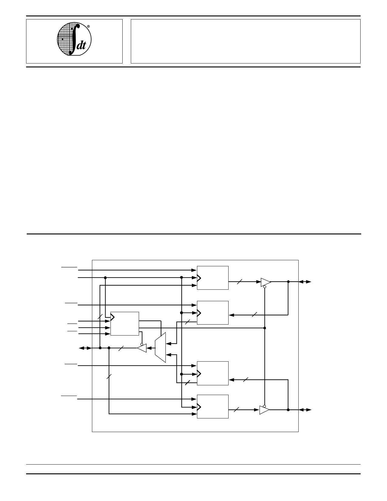
FUNCTIONAL BLOCK DIAGRAM
CEA1B
CLK
CE1B
SEL
OEB
OEA
A1:12
CE2B
12
CONTROL
REGISTER
12
12
M1
U
X0
CEA2B
CE A-1B
REGISTER
Q
D
12
CE 1B-A
REGISTER
D
Q
12
12
CE 2B-A
REGISTER
Q
12
D
12
CE A-2B
REGISTER
Q
D
12
1B1:12
2B1:12
The IDT logo is a registered trademark of Integrated Device Technology, Inc.
MILITARY AND COMMERCIAL TEMPERATURE RANGES
©1996 Integrated Device Technology, Inc.
5.5
3071 drw 01
AUGUST 1996
DSC-3071/3
1
1 page 
IDT54/74FCT162H272AT/CT/ET
FAST CMOS 12-BIT SYNCHRONOUS TRI-PORT BUS EXCHANGER
MILITARY AND COMMERCIAL TEMPERATURES RANGES
POWER SUPPLY CHARACTERISTICS
Symbol
Parameter
Test Conditions(1)
Min. Typ.(2) Max. Unit
∆ICC
Quiescent Power Supply Current VCC = Max.
TTL Inputs HIGH
VIN = 3.4V(3)
— 0.5 1.5 mA
ICCD
Dynamic Power Supply Current(4) VCC = Max.
VIN = VCC
— 60 100 µA/
Outputs Open
VIN = GND
MHz
One Output Port Enabled
CExx = GND
One Input Bit Toggling
One Output Bit Toggling
50% Duty Cycle
IC
Total Power Supply Current(6)
VCC = Max.
VIN = VCC
— 0.6 1.5 mA
Outputs Open
VIN = GND
fi = 10MHz
50% Duty Cycle
VIN = 3.4V
— 0.9 2.3
One Output Port Enabled
CExx = GND
VIN = GND
One Input Bit Toggling
One Output Bit Toggling
VCC = Max.
VIN = VCC
— 1.8 3.5(5)
Outputs Open
VIN = GND
fi = 2.5MHz
50% Duty Cycle
VIN = 3.4V
— 4.8 12.5(5)
One Output Port Enabled
CExx = GND
VIN = GND
Twelve Input Bits Toggling
Twelve Output Bits Toggling
NOTES:
3071 tbl 09
1. For conditions shown as Max. or Min., use appropriate value specified under Electrical Characteristics for the applicable device type.
2. Typical values are at VCC = 5.0V, +25°C ambient.
3. Per TTL driven input (VIN = 3.4V). All other inputs at VCC or GND.
4. This parameter is not directly testable, but is derived for use in Total Power Supply Calculations.
5. Values for these conditions are examples of the ICC formula. These limits are guaranteed but not tested.
6. IC = IQUIESCENT + IINPUTS + IDYNAMIC
IC = ICC + ∆ICC DHNT + ICCD (fCPNCP/2 + fiNi)
ICC = Quiescent Current (ICCL, ICCH and ICCZ)
∆ICC = Power Supply Current for a TTL High Input (VIN = 3.4V)
DH = Duty Cycle for TTL Inputs High
NT = Number of TTL Inputs at DH
ICCD = Dynamic Current Caused by an Input Transition Pair (HLH or LHL)
fCP = Clock Frequency for Register Devices (Zero for Non-Register Devices)
NCP = Number of Clock Inputs at fCP
fi = Input Frequency
Ni = Number of Inputs at fi
5.5 5
5 Page | ||
| Páginas | Total 8 Páginas | |
| PDF Descargar | [ Datasheet IDT54FCT162H272.PDF ] | |
Hoja de datos destacado
| Número de pieza | Descripción | Fabricantes |
| IDT54FCT162H272 | FAST CMOS 12-BIT SYNCHRONOUS BUS EXCHANGER | Integrated Device Technology |
| Número de pieza | Descripción | Fabricantes |
| SLA6805M | High Voltage 3 phase Motor Driver IC. |
Sanken |
| SDC1742 | 12- and 14-Bit Hybrid Synchro / Resolver-to-Digital Converters. |
Analog Devices |
|
DataSheet.es es una pagina web que funciona como un repositorio de manuales o hoja de datos de muchos de los productos más populares, |
| DataSheet.es | 2020 | Privacy Policy | Contacto | Buscar |