|
|
|
PDF DT72V3674L10PF Data sheet ( Hoja de datos )
| Número de pieza | DT72V3674L10PF | |
| Descripción | 3.3 VOLT CMOS SyncBiFIFOTM WITH BUS-MATCHING 2/048 x 36 x 2 4/096 x 36 x 2 8/192 x 36 x 2 | |
| Fabricantes | Integrated Device Technology | |
| Logotipo | ||
Hay una vista previa y un enlace de descarga de DT72V3674L10PF (archivo pdf) en la parte inferior de esta página. Total 30 Páginas | ||
|
No Preview Available !
3.3 VOLT CMOS SyncBiFIFOTM WITH BUS-MATCHING
2,048 x 36 x 2
4,096 x 36 x 2
8,192 x 36 x 2
IDT72V3654
IDT72V3664
IDT72V3674
FEATURES
• Memory storage capacity:
IDT72V3654 – 2,048 x 36 x 2
IDT72V3664 – 4,096 x 36 x 2
IDT72V3674 – 8,192 x 36 x 2
• Clock frequencies up to 100 MHz (6.5ns access time)
• Two independent clocked FIFOs buffering data in opposite
directions
• Select IDT Standard timing (using EFA, EFB, FFA, and FFB flags
functions) or First Word Fall Through Timing (using ORA, ORB,
IRA, and IRB flag functions)
• Programmable Almost-Empty and Almost-Full flags; each has five
default offsets (8, 16, 64, 256 and 1,024 )
• Serial or parallel programming of partial flags
• Port B bus sizing of 36 bits (long word), 18 bits (word) and 9 bits
(byte)
• Big- or Little-Endian format for word and byte bus sizes
• Retransmit Capability
• Master Reset clears data and configures FIFO, Partial Reset
clears data but retains configuration settings
• Mailbox bypass registers for each FIFO
• Free-running CLKA and CLKB may be asynchronous or coincident
(simultaneous reading and writing of data on a single clock edge
is permitted)
• Auto power down minimizes power dissipation
• Available in space saving 128-pin Thin Quad Flatpack (TQFP)
• Pin and functionally compatible version of the 5V operating
IDT723654/723664/723674
• Pin compatible to the lower density parts, IDT72V3624/72V3634/
72V3644
• Industrial temperature range (–40°C to +85°C) is available
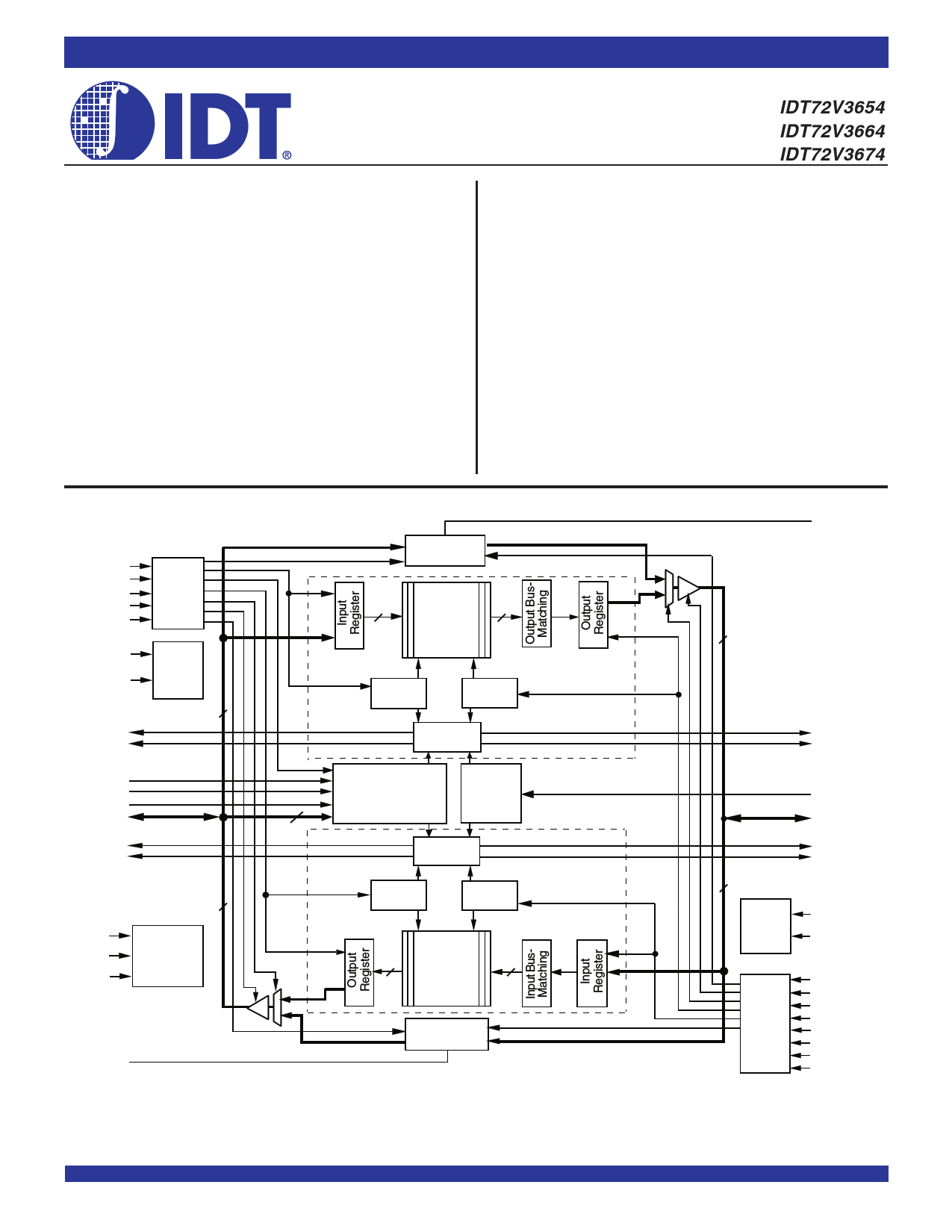
FUNCTIONAL BLOCK DIAGRAM
CLKA
CSA
W/RA
ENA
MBA
MRS1
PRS1
FFA/IRA
AFA
Port-A
Control
Logic
FIFO1,
Mail1
Reset
Logic
36
Mail 1
Register
36
RAM ARRAY
2,048 x 36
36
4,096 x 36
8,192 x 36
FIFO1
Write
Pointer
Read
Pointer
Status Flag
Logic
MBF1
36
EFB/ORB
AEB
FS2
FS0/SD
FS1/SEN
A0-A35
EFA/ORA
AEA
Programmable Flag
Offset Registers
Timing
Mode
13
FIFO2
Status Flag
Logic
FWFT
B0-B35
FFB/IRB
AFB
RT1
RTM
RT2
36
FIFO1 and
FIFO2
Retransmit
Logic
MBF2
Read
Pointer
Write
Pointer
RAM ARRAY
36 2,048 x 36
4,096 x 36
8,192 x 36
Mail 2
Register
36
36
FIFO2,
Mail2
Reset
Logic
MRS2
PRS2
Port-B
Control
Logic
CLKB
CSB
W/RB
ENB
MBB
BE
BM
SIZE
4664 drw01
IDT and the IDT logo are registered trademarks of Integrated Device Technology, Inc. The SyncFIFO is a trademark of Integrated Device Technology, Inc.
COMMERCIAL TEMPERATURE RANGE
1
2003 Integrated Device Technology, Inc. All rights reserved. Product specifications subject to change without notice.
NOVEMBER 2003
DSC-4664/4
1 page 
IDT72V3654/72V3664/72V3674 3.3V CMOS SyncBiFIFOTM WITH BUS-MATCHING
2,048 x 36 x 2, 4,096 x 36 x 2 and 8,192 x 36 x 2
COMMERCIALTEMPERATURERANGE
PIN DESCRIPTIONS (CONTINUED)
Symbol
FS0/SD
Name
Flag Offset Select 0/
Serial Data
I/O
I
FS1/SEN FlagOffsetSelect1/
Serial Enable,
FS2(1)
Flag Offset Select 2
I
I
MBA Port A Mailbox
Select
I
Description
FS1/SENand FS0/SD are dual-purpose inputs used for flag offset register programming. During
Master Reset, FS1/SENand FS0/SD, together with FS2, select the flag offset programming method
Three offset register programming methods are available: automatically load one of five preset values
(8, 16, 64, 256 or 1,024), parallel load from Port A, and serial load.
When serial load is selected for flag offset register programming, FS1/SENis used as an enable
synchronous to the LOW-to-HIGH transition of CLKA. When FS1/SENis LOW, a rising edge on CLKA
load the bit present on FS0/SD into the X and Y registers. The number of bit writes required to program
the offset registers is 44 for the IDT72V3654, 48 for the IDT72V3664, and 52 for the IDT72V3674.
The first bit write stores the Y-register (Y1) MSB and the last bit write stores the X-register (X2) LSB.
A HIGH level on MBA chooses a mailbox register for a Port A read or write operation. When
the A0-A35 outputs are active, a HIGH level on MBA selects data from the mail2 register for output
and a LOW level selects FIFO2 output register data for output.
MBB Port B Mailbox
Select
I A HIGH level on MBB chooses a mailbox register for a Port B read or write operation. When the
B0-B35 outputs are active, a HIGH level on MBB selects data from the mail1 register for output and
a LOW level selects FIFO1 output register data for output.
MBF1
MBF2
MRS1
MRS2
PRS1/
RT1
Mail1 Register
Flag
Mail2 Register
Flag
FIFO1 Master
Reset
FIFO2 Master
Reset
Partial Reset/
Retransmit FIFO1
O MBF1 is set LOW by a LOW-to-HIGH transition of CLKA that writes data to the mail1 register.
Writes to the mail1 register are inhibited while MBF1 is LOW. MBF1 is set HIGH by a LOW-to-HIGH
transition of CLKB when a Port B read is selected and MBB is HIGH. MBF1 is set HIGH following either
a Master or Partial Reset of FIFO1.
O MBF2is set LOW by a LOW-to-HIGH transition of CLKB that writes data to the mail2 register. Writes
to the mail2 register are inhibited while MBF2is LOW. MBF2 is set HIGH by a LOW-to-HIGH
transition of CLKA when a Port A read is selected and MBA is HIGH. MBF2 is set HIGH following
either a Master or Partial Reset of FIFO2.
I A LOW on this pin initializes the FIFO1 read and write pointers to the first location of memory and sets the
Port B output register to all zeroes. A LOW-to-HIGH transition on MRS1 selects the programming
method (serial or parallel) and one of five programmable flag default offsets for FIFO1 and FIFO2. It
also configures Port B for bus size and endian arrangement. Four LOW-to-HIGH transitions of CLKA
and four LOW-to-HIGH transitions of CLKB must occur while MRS1is LOW.
I A LOW on this pin initializes the FIFO2 read and write pointers to the first location of memory and sets
the Port A output register to all zeroes. A LOW-to-HIGH transition on MRS2, toggled simultaneously with
MRS1, selects the programming method (serial or parallel) and one of the programmable flag default
offsets for FIFO2. Four LOW-to-HIGH transitions of CLKA and four LOW-to-HIGH transitions of CLKB
must occur while MRS2is LOW.
I This pin is muxed for both Partial Reset and Retransmit operations, it is used in conjunction with the RTM
pin. If RTM is in a LOW condition, a LOW on this pin performs a Partial Reset on FIFO1 and initializes
the FIFO1 read and write pointers to the first location of memory and sets the Port B output register to
all zeroes. During Partial Reset, the currently selected bus size, endian arrangement, programming
method (serial or parallel), and programmable flag settings are all retained. If RTM is HIGH, a LOW on
this pin performs a Retransmit and initializes the FIFO1 read pointer only to the first memory location.
PRS2/
RT2
Partial Reset/
Retransmit FIFO2
I This pin is muxed for both Partial Reset and Retransmit operations, it is used in conjunction with the RTM
pin. If RTMis in a LOW condition, a LOW on this pin performs a Partial Reset on FIFO2 and initializes
the FIFO2 read and write selected bus size, endian arrangement, programming method (serial or
parallel), and programmable flag settings are all retained. If RTM is HIGH, a LOW on this pin performs
a Retransmit and initializes the FIFO2 read pointer only to the first memory location.
RTM
Retransmit Mode
I This pin is used in conjunction with the RT1 and RT2 pins. When RTM is HIGH a Retransmit is performed
on FIFO1 or FIFO2 respectively.
SIZE(1)
Bus Size Select
I A HIGH on this pin when BM is HIGH selects byte bus (9-bit) size on Port B. A LOW on this pin when
BM is HIGH selects word (18-bit) bus size. SIZE works with BM and BE to select the bus size and endian
arrangement for Port B. The level of SIZE must be static throughout device operation
NOTE:
1. FS2, BM and SIZE inputs are not TTL compatible. These inputs should be tied to GND or VCC.
5
5 Page 
IDT72V3654/72V3664/72V3674 3.3V CMOS SyncBiFIFOTM WITH BUS-MATCHING
2,048 x 36 x 2, 4,096 x 36 x 2 and 8,192 x 36 x 2
COMMERCIALTEMPERATURERANGE
SIGNAL DESCRIPTION
MASTER RESET (MRS1, MRS2)
Afterpowerup,aMasterReset operationmustbeperformedbyproviding
a LOW pulse to MRS1 and MRS2 simultaneously. Afterwards, each of the
two FIFO memories of the IDT72V3654/72V3664/72V3674 undergoes a
complete reset by taking its associated Master Reset (MRS1, MRS2) input
LOW for at least four Port A Clock (CLKA) and four Port B Clock (CLKB) LOW-
to-HIGH transitions. The Master Reset inputs can switch asynchronously to
theclocks.AMasterReset initializestheassociatedwriteandreadpointersto
the first location of the memory and forces the Full/Input Ready flag (FFA/IRA,
FFB/IRB) LOW, the Empty/Output Ready flag (EFA/ORA, EFB/ORB) LOW,
the Almost-Empty flag (AEA, AEB) LOW and forces the Almost-Full flag
(AFA, AFB) HIGH. A Master Reset also forces the associated Mailbox Flag
(MBF1, MFB2) of the parallel mailbox register HIGH. After a Master Reset,
theFIFO'sFull/InputReadyflagissetHIGHaftertwowriteclockcycles. Then
the FIFO is ready to be written to.
A LOW-to-HIGH transition on the FIFO1 Master Reset (MRS1) input
latches the values of the Big-Endian (BE) input for determining the order by
which bytes are transferred through Port B. It also latches the values of the
Flag Select (FS0, FS1 and FS2) inputs for choosing the Almost-Full and Almost-
Empty offset programming method.
A LOW-to-HIGH transition on the FIFO2 Master Reset (MRS2) clears
theFlagOffsetRegistersofFIFO2(X2,Y2). ALOW-to-HIGHtransitiononthe
FIFO2 Master Reset (MRS2) together with the FIFO1 Master Reset (MRS1)
input latches the value of the Big-Endian (BE) input for Port B and also latches
the values of the Flag Select (FS0, FS1 and FS2) inputs for choosing the Almost-
Full and Almost-Empty offset programming method. (For details see Table 1,
Flag Programming, and the Programming the Almost-Empty and Almost-Full
Flags section). The relevant FIFO Master Reset timing diagram can be found
in Figure 3.
PARTIAL RESET (PRS1, PRS2)
Each of the two FIFO memories of these devices undergoes a limited reset
by taking its associated Partial Reset (PRS1, PRS2) input LOW for at least
four Port A Clock (CLKA) and four Port B Clock (CLKB) LOW-to-HIGH
transitions. The PartialReset inputscan switch asynchronouslyto the clocks.
A Partial Reset initializes the internal read and write pointers and forces the
Full/Input Ready flag (FFA/IRA, FFB/IRB) LOW, the Empty/Output Ready
flag (EFA/ORA, EFB/ORB) LOW, the Almost-Empty flag (AEA, AEB)
LOW, and the Almost-Full flag (AFA, AFB) HIGH. A Partial Reset also forces
the Mailbox Flag (MBF1, MBF2) of the parallel mailbox register HIGH. After
a Partial Reset, the FIFO’s Full/Input Ready flag is set HIGH after two write
clock cycles. Then the FIFO is ready to be written to.
Whatever flag offsets, programming method (parallel or serial), and timing
mode (FWFT or IDT Standard mode) are currently selected at the time a Partial
Reset is initiated, those settings will be remain unchanged upon completion of
the reset operation. A Partial Reset may be useful in the case where
reprogramming a FIFO following a Master Reset would be inconvenient. See
Figure 4 for the Partial Reset timing diagram.
RETRANSMIT (RT1, RT2)
The FIFO1 memory of these devices undergoes a Retransmit by taking its
associated Retransmit (RT1) input LOW for at least four Port A Clock (CLKA)
and four Port B Clock (CLKB) LOW-to-HIGH transitions. The Retransmit
initializes the read pointer of FIFO1 to the first memory location.
The FIFO2 memory undergoes a Retransmit by taking its associated
Retransmit (RT2) input LOW for at least four Port A Clock (CLKA) and four Port
C Clock (CLKC) LOW-to-HIGH transitions. The Retransmit initializes the read
pointer of FIFO2 to the first memory location.
The RTM pin must be HIGH during the time of Retranmit. Note that the
RT1input is muxed with thePRS1input, the state of the RTM pin determining
whether this pin performs a Retransmit or Partial Reset. Also, the RT2inputis
muxedwiththePRS2 input,thestateoftheRTMpindeterminingwhetherthis
pin performs a Retransmit or Partial Reset.
BIG-ENDIAN/FIRST WORD FALL THROUGH (BE/FWFT)
— ENDIAN SELECTION
This is a dual purpose pin. At the time of Master Reset, the BE select function
is active, permitting a choice of Big or Little-Endian byte arrangement for data
written to or read from Port B. This selection determines the order by which
bytes (or words) of data are transferred through this port. For the following
illustrations, assume that a byte (or word) bus size has been selected for Port
B. (Note that when Port B is configured for a long word size, the Big-Endian
function has no application and the BE input is a “don’t care”1.)
A HIGH on the BE/FWFT input when the Master Reset (MRS1, MRS2)
inputs go from LOW to HIGH will select a Big-Endian arrangement. When data
is moving in the direction from Port A to Port B, the most significant byte (word)
of the long word written to Port A will be read from Port B first; the least significant
byte (word) of the long word written to Port A will be read from Port B last. When
data is moving in the direction from Port B to Port A, the byte (word) written
to Port B first will be read from Port A as the most significant byte (word) of the
long word; the byte (word) written to Port B last will be read from Port A as
the least significant byte (word) of the long word.
A LOW on the BE/FWFT input when the Master Reset (MRS1, MRS2)
inputs go from LOW to HIGH will select a Little-Endian arrangement. When data
is moving in the direction from Port A to Port B, the least significant byte (word)
of the long word written to Port A will be read from Port B first; the most significant
byte (word) of the long word written to Port A will be read from Port B last. When
data is moving in the direction from Port B to Port A, the byte (word) written
to Port B first will be read from Port A as the least significant byte (word) of the
long word; the byte (word) written to Port B last will be read from Port A as
the most significant byte (word) of the long word. Refer to Figure 2 for an
illustration of the BE function. See Figure 3 (Master Reset) for the Endian select
timing diagram.
— TIMING MODE SELECTION
After Master Reset, the FWFT select function is active, permitting a choice
between two possible timing modes: IDT Standard mode or First Word Fall
Through (FWFT) mode. Once the Master Reset (MRS1, MRS2) input is
HIGH, a HIGH on the BE/FWFT input during the next LOW-to-HIGH
transition of CLKA (for FIFO1) and CLKB (for FIFO2) will select IDT Standard
mode. This mode uses the Empty Flag function (EFA, EFB) to indicate
whether or not there are any words present in the FIFO memory. It uses the
Full Flag function (FFA, FFB) to indicate whether or not the FIFO memory
has any free space for writing. In IDT Standard mode, every word read from
the FIFO, including the first, must be requested using a formal read operation.
NOTE:
1. Either a HIGH or LOW can be applied to a "don't care" input with no change to the logical operation of the FIFO. Nevertheless, inputs that are temporarily "don't care" (along with
unused inputs) must not be left open, rather they must be either HIGH or LOW.
11
11 Page | ||
| Páginas | Total 30 Páginas | |
| PDF Descargar | [ Datasheet DT72V3674L10PF.PDF ] | |
Hoja de datos destacado
| Número de pieza | Descripción | Fabricantes |
| DT72V3674L10PF | 3.3 VOLT CMOS SyncBiFIFOTM WITH BUS-MATCHING 2/048 x 36 x 2 4/096 x 36 x 2 8/192 x 36 x 2 | Integrated Device Technology |
| Número de pieza | Descripción | Fabricantes |
| SLA6805M | High Voltage 3 phase Motor Driver IC. |
Sanken |
| SDC1742 | 12- and 14-Bit Hybrid Synchro / Resolver-to-Digital Converters. |
Analog Devices |
|
DataSheet.es es una pagina web que funciona como un repositorio de manuales o hoja de datos de muchos de los productos más populares, |
| DataSheet.es | 2020 | Privacy Policy | Contacto | Buscar |