|
|
|
PDF EL5421C Data sheet ( Hoja de datos )
| Número de pieza | EL5421C | |
| Descripción | Quad 12MHz Rail-to-Rail Input-Output Buffer | |
| Fabricantes | Elantec Semiconductor | |
| Logotipo | ||
Hay una vista previa y un enlace de descarga de EL5421C (archivo pdf) en la parte inferior de esta página. Total 13 Páginas | ||
|
No Preview Available !
EL5421C
Quad 12MHz Rail-to-Rail Input-Output Buffer
Features
• 12MHz -3dB Bandwidth
• Unity gain buffer
• Supply voltage = 4.5V to 16.5V
• Low supply current (per buffer) =
500µ A
• High slew rate = 10V/µs
• Rail to Rail operation
• “Mini” SO Package (MSOP)
Applications
• TFT-LCD Drive Circuits
• Electronics Notebooks
• Electronics Games
• Personal Communication Devices
• Personal Digital Assistants (PDA)
• Portable Instrumentation
• Wireless LANs
• Office Automation
• Active Filters
• ADC/DAC Buffer
Ordering Information
Part No.
EL5421CY
Temp. Range
Package
-40°C to +85°C 10-Pin MSOP
Outline #
MDP0043
General Description
The EL5421C is a quad, low power, high voltage rail-to-rail input-out-
put buffer. Operating on supplies ranging from 5V to 15V, while
consuming only 500µA per channel, the EL5421C has a bandwidth of
12MHz (-3dB). The EL5421C also provides rail-to-rail input and out-
put ability, giving the maximum dynamic range at any supply voltage.
The EL5421C also features fast slewing and settling times, as well as
a high output drive capability of 30mA (sink and source). These fea-
tures make the EL5421C ideal for use as voltage reference buffers in
Thin Film Transistor Liquid Crystal Displays (TFT-LCD). Other
applications include battery power, portable devices and anywhere
low power consumption is important.
The EL5421C is available in a space saving 10-Pin MSOP package
and operates over a temperature range of -40°C to +85°C.
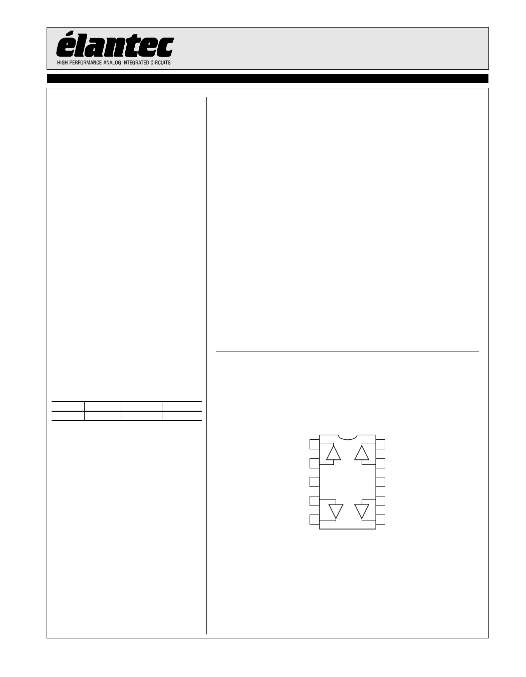
Connection Diagram
VOUTA 1
VINA 2
VS+ 3
VINB 4
VOUTB 5
10 VOUTD
9 VIND
8 VS-
7 VINC
6 VOUTC
EL 5421C (MSOP 10)
© 2000 Elantec Semiconductor, Inc.
1 page 
EL5421C
Quad 12MHz Rail-to-Rail Input-Output Buffer
Typical Performance Curves
Input Offset Voltage Distribution
1800
1600 VS=±5V
1400 TA=25°C
1200
Typical
Production
Distribution
1000
800
600
400
200
0
Input Offset Voltage (mV)
Input Offset Voltage vs Temperature
10
VS=± 5V
5
0
-5
-50 0 50 100
Temperature (°C)
Output High Voltage vs Temperature
4.97
150
VS=± 5V
4.96 IOUT=5mA
4.95
4.94
4.93
-50
0 50 100
Temperature (°C)
150
Input Offset Voltage Drift
70
VS=±5V
60
50
40
30
20
10
0
Typical
Production
Distribution
Input Offset Voltage Drift, TCVOS(µ V/°C)
Input Bias Current vs Temperature
2.0
VS=±5V
0.0
-2.0
-50 0 50 100
Temperature (°C)
Output Low Voltage vs Temperature
-4.91
-4.92
VS=± 5V
-4.93 IOUT=-5mA
-4.94
-4.95
-4.96
-4.97
-50
0 50 100
Temperature (°C)
150
150
5
5 Page 
EL5421C
Quad 12MHz Rail-to-Rail Input-Output Buffer
maximum junction temperature for the application to
determine if load conditions need to be modified for the
buffer to remain in the safe operating area.
The maximum power dissipation allowed in a package is
determined according to:
PDMAX = T----J---M-----A----X--Θ---–--J--A-T----A----M-----A----X--
where:
TJMAX = Maximum Junction Temperature
TAMAX= Maximum Ambient Temperature
θJA = Thermal Resistance of the Package
PDMAX = Maximum Power Dissipation in the
Package
The maximum power dissipation actually produced by
an IC is the total quiescent supply current times the total
power supply voltage, plus the power in the IC due to the
loads, or:
PDMAX = Σi[V S × ISMAX + (V S+ – VOUTi ) × ILOADi ]
when sourcing, and:
PDMAX = Σi[VS × ISMAX + (VOUTi – VS- ) × ILOADi ]
when sinking.
Where:
i = 1 to 4 for Quad
VS = Total Supply Voltage
ISMAX = Maximum Supply Current Per Channel
VOUTi = Maximum Output Voltage of the
Application
ILOADi = Load current
If we set the two PDMAX equations equal to each other,
we can solve for RLOADi to avoid device overheat. Fig-
ure 3 and Figure 4 provide a convenient way to see if the
device will overheat. The maximum safe power dissipa-
tion can be found graphically, based on the package type
and the ambient temperature. By using the previous
equation, it is a simple matter to see if PDMAX exceeds
the device’s power derating curves. To ensure proper
operation, it is important to observe the recommended
derating curves shown in Figure 3 and Figure 4.
MSOP10 Package Mounted on JEDEC JESD51-7
High Effective Thermal Conductivity Test Board
1200
1000
870mW
MAX TJ=125°C
800
600 MSOP10---- Θ
400 JA =115°C/W
200
0
0 25 50 75 85 100 125 150
Ambient Temperature (°C)
Figure 3. Package Power Dissipation vs
Ambient Temperature
MSOP10 Package Mounted on JEDEC JESD51-3
Low Effective Thermal Conductivity Test Board
600
500 485mW
400
300 MSOP10---Θ
200 JA =206°C/W
100
MAX TJ=125°C
0
0 25 50 75 85 100 125 150
Ambient Temperature (°C)
Figure 4. Package Power Dissipation vs
Ambient Temperature
Unused Buffers
It is recommended that any unused buffer have the input
tied to the ground plane.
11
11 Page | ||
| Páginas | Total 13 Páginas | |
| PDF Descargar | [ Datasheet EL5421C.PDF ] | |
Hoja de datos destacado
| Número de pieza | Descripción | Fabricantes |
| EL5421 | Quad 12MHz Rail-to-Rail Input-Output Buffer | Intersil |
| EL5421C | Quad 12MHz Rail-to-Rail Input-Output Buffer | Elantec Semiconductor |
| EL5421T | 12MHz Rail-to-Rail Input-Output Buffer | Intersil Corporation |
| Número de pieza | Descripción | Fabricantes |
| SLA6805M | High Voltage 3 phase Motor Driver IC. |
Sanken |
| SDC1742 | 12- and 14-Bit Hybrid Synchro / Resolver-to-Digital Converters. |
Analog Devices |
|
DataSheet.es es una pagina web que funciona como un repositorio de manuales o hoja de datos de muchos de los productos más populares, |
| DataSheet.es | 2020 | Privacy Policy | Contacto | Buscar |