|
|
|
PDF M25P80 Data sheet ( Hoja de datos )
| Número de pieza | M25P80 | |
| Descripción | 8 Mbit/ Low Voltage/ Serial Flash Memory With 25 MHz SPI Bus Interface | |
| Fabricantes | STMicroelectronics | |
| Logotipo | ||
Hay una vista previa y un enlace de descarga de M25P80 (archivo pdf) en la parte inferior de esta página. Total 30 Páginas | ||
|
No Preview Available !
M25P80
8 Mbit, Low Voltage, Serial Flash Memory
With 25 MHz SPI Bus Interface
PRELIMINARY DATA
FEATURES SUMMARY
s 8 Mbit of Flash Memory
s Page Program (up to 256 Bytes) in 1.5ms
(typical)
s Sector Erase (512 Kbit) in 2 s (typical)
s Bulk Erase (8 Mbit) in 10 s (typical)
s 2.7 V to 3.6 V Single Supply Voltage
s SPI Bus Compatible Serial Interface
s 25 MHz Clock Rate (maximum)
s Deep Power-down Mode 1 µA (typical)
s Electronic Signature (13h)
s More than 100,000 Erase/Program Cycles per
Sector
s More than 20 Year Data Retention
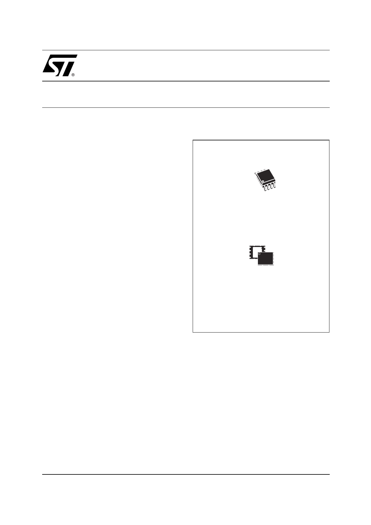
Figure 1. Packages
8
1
SO8 (MW)
200 mil width
VFQFPN8 (MP)
(MLP8)
December 2002
This is preliminary information on a new product now in development or undergoing evaluation. Details are subject to change without notice.
1/35
1 page 
M25P80
OPERATING FEATURES
Page Programming
To program one data byte, two instructions are re-
quired: Write Enable (WREN), which is one byte,
and a Page Program (PP) sequence, which con-
sists of four bytes plus data. This is followed by the
internal Program cycle (of duration tPP).
To spread this overhead, the Page Program (PP)
instruction allows up to 256 bytes to be pro-
grammed at a time (changing bits from 1 to 0), pro-
vided that they lie in consecutive addresses on the
same page of memory.
Sector Erase and Bulk Erase
The Page Program (PP) instruction allows bits to
be reset from 1 to 0. Before this can be applied, the
bytes of memory need to have been erased to all
1s (FFh). This can be achieved either a sector at a
time, using the Sector Erase (SE) instruction, or
throughout the entire memory, using the Bulk
Erase (BE) instruction. This starts an internal
Erase cycle (of duration tSE or tBE).
The Erase instruction must be preceeded by a
Write Enable (WREN) instruction.
Polling During a Write, Program or Erase Cycle
A further improvement in the time to Write Status
Register (WRSR), Program (PP) or Erase (SE or
BE) can be achieved by not waiting for the worst
case delay (tW, tPP, tSE, or tBE). The Write In
Progress (WIP) bit is provided in the Status Regis-
ter so that the application program can monitor its
value, polling it to establish when the previous
Write cycle, Program cycle or Erase cycle is com-
plete.
Active Power, Stand-by Power and Deep
Power-Down Modes
When Chip Select (S) is Low, the device is en-
abled, and in the Active Power mode.
When Chip Select (S) is High, the device is dis-
abled, but could remain in the Active Power mode
until all internal cycles have completed (Program,
Erase, Write Status Register). The device then
goes in to the Stand-by Power mode. The device
consumption drops to ICC1.
The Deep Power-down mode is entered when the
specific instruction (the Enter Deep Power-down
Mode (DP) instruction) is executed. The device
consumption drops further to ICC2. The device re-
mains in this mode until another specific instruc-
tion (the Release from Deep Power-down Mode
and Read Electronic Signature (RES) instruction)
is executed.
All other instructions are ignored while the device
is in the Deep Power-down mode. This can be
used as an extra software protection mechanism,
when the device is not in active use, to protect the
device from inadvertant Write, Program or Erase
instructions.
Status Register
The Status Register contains a number of status
and control bits that can be read or set (as appro-
priate) by specific instructions.
WIP bit. The Write In Progress (WIP) bit indicates
whether the memory is busy with a Write Status
Register, Program or Erase cycle.
WEL bit. The Write Enable Latch (WEL) bit indi-
cates the status of the internal Write Enable Latch.
BP2, BP1, BP0 bits. The Block Protect (BP2,
BP1, BP0) bits are non-volatile. They define the
size of the area to be software protected against
Program and Erase instructions.
SRWD bit. The Status Register Write Disable
(SRWD) bit is operated in conjunction with the
Write Protect (W) signal. The Status Register
Write Disable (SRWD) bit and Write Protect (W)
signal allow the device to be put in the Hardware
Protected mode. In this mode, the non-volatile bits
of the Status Register (SRWD, BP2, BP1, BP0)
become read-only bits.
5/35
5 Page 
Figure 8. Write Enable (WREN) Instruction Sequence
S
01234567
C
Instruction
D
High Impedance
Q
AI02281E
M25P80
Write Enable (WREN)
The Write Enable (WREN) instruction (Figure 8)
sets the Write Enable Latch (WEL) bit.
The Write Enable Latch (WEL) bit must be set pri-
or to every Page Program (PP), Sector Erase
(SE), Bulk Erase (BE) and Write Status Register
(WRSR) instruction.
The Write Enable (WREN) instruction is entered
by driving Chip Select (S) Low, sending the in-
struction code, and then driving Chip Select (S)
High.
Figure 9. Write Disable (WRDI) Instruction Sequence
S
01234567
C
Instruction
D
High Impedance
Q
AI03750D
Write Disable (WRDI)
The Write Disable (WRDI) instruction (Figure 9)
resets the Write Enable Latch (WEL) bit.
The Write Disable (WRDI) instruction is entered by
driving Chip Select (S) Low, sending the instruc-
tion code, and then driving Chip Select (S) High.
The Write Enable Latch (WEL) bit is reset under
the following conditions:
– Power-up
– Write Disable (WRDI) instruction completion
– Write Status Register (WRSR) instruction com-
pletion
– Page Program (PP) instruction completion
– Sector Erase (SE) instruction completion
– Bulk Erase (BE) instruction completion
11/35
11 Page | ||
| Páginas | Total 30 Páginas | |
| PDF Descargar | [ Datasheet M25P80.PDF ] | |
Hoja de datos destacado
| Número de pieza | Descripción | Fabricantes |
| M25P80 | 8 Mbit/ Low Voltage/ Serial Flash Memory With 25 MHz SPI Bus Interface | STMicroelectronics |
| M25P80 | 8Mb (1Mb x 8) serial Flash memory device | Micron |
| Número de pieza | Descripción | Fabricantes |
| SLA6805M | High Voltage 3 phase Motor Driver IC. |
Sanken |
| SDC1742 | 12- and 14-Bit Hybrid Synchro / Resolver-to-Digital Converters. |
Analog Devices |
|
DataSheet.es es una pagina web que funciona como un repositorio de manuales o hoja de datos de muchos de los productos más populares, |
| DataSheet.es | 2020 | Privacy Policy | Contacto | Buscar |