|
|
|
PDF DS75107 Data sheet ( Hoja de datos )
| Número de pieza | DS75107 | |
| Descripción | Dual Line Receiver | |
| Fabricantes | National Semiconductor | |
| Logotipo | ||
Hay una vista previa y un enlace de descarga de DS75107 (archivo pdf) en la parte inferior de esta página. Total 9 Páginas | ||
|
No Preview Available !
May 1999
DS75107
Dual Line Receiver
General Description
The product described herein is a TTL compatible dual high
speed circuit intended for sensing in a broad range of system
applications. While the primary usage will be for line receiv-
ers of MOS sensing, the product may effectively be used as
a voltage comparator, level translator, window detector,
transducer preamplifier, and in other sensing applications.
As a digital line receiver the product is applicable with the
SN55109/SN75109 and µA75110/DS75110 companion driv-
ers, or may be used in other balanced or unbalanced
party-line data transmission systems.
Input protection diodes are incorporated in series with the
collectors of the differential input stage. These diodes are
useful in certain applications that have multiple VCC+ sup-
plies or VCC+ supplies that are turned off.
Features
n Diode protected input stage for power “OFF” condition
n 17 ns typ high speed
n TTL compatible
n ±10 mV or ±25 mV input sensitivity
n ±3V input common-mode range
n High input impedance with normal VCC, or VCC = 0V
n Strobes for channel selection
n Dual circuits
n Sensitivity gntd. over full common-mode range
n Logic input clamp diodes — meets both “A” and “B”
version specifications
n ±5V standard supply voltages
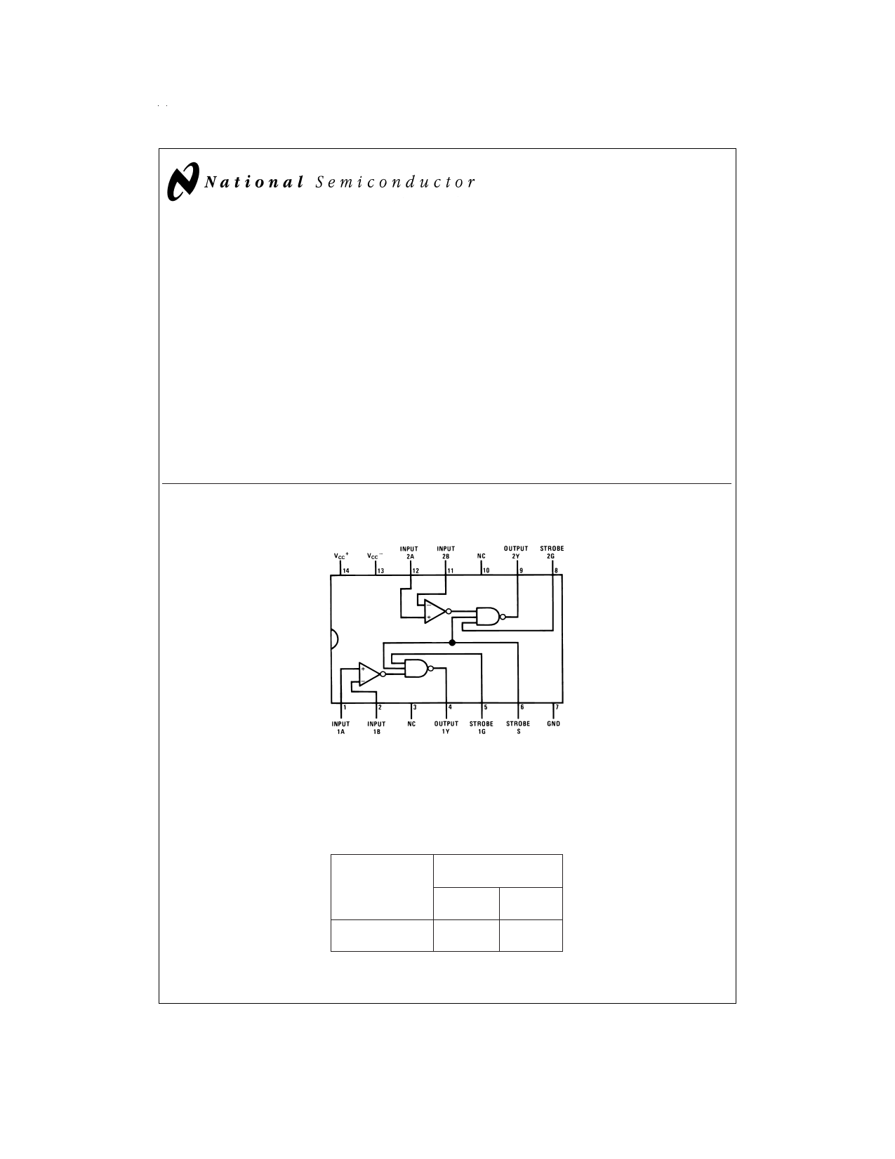
Connection Diagram
Dual-In-Line Package
DS009446-1
Top View
Order Number DS75107M, DS75107N
See NS Package Number M14A or N14A
For Complete Military 883 Specifications, see RETS Datasheet.
Order Number DS55107AJ/883
See NS Package Number J14A
Selection Guide
Temperature→
Package→
Input Sensitivity→
Output Logic↓
TTL Active Pull-Up
TTL Open Collector
0˚C ≤ TA ≤ +70˚C
Cavity or Molded Dip
±25 mV
±10 mV
DS75107
© 1999 National Semiconductor Corporation DS009446
www.national.com
1 page 
Typical Applications (Continued)
The strobe feature of the receiver and the inhibit feature of
the driver allows the DS75107 dual line circuit to be used in
data-bus or party-line systems. In these applications, several
drivers and receivers may share a common transmission
line. An enabled driver transmits data to all enabled receiv-
ers on the line while other drivers and receivers are disabled.
Data is thus time multiplexed on the transmission line.
DS75107 device specifications allow widely varying thermal
and electrical environments at the various driver and re-
ceiver locations. The data-bus system offers maximum per-
formance at minimum cost.
The DS75107 dual line circuits may also be used in unbal-
anced or single line systems. Although these systems do not
offer the same performance as balanced systems for long
lines, they are adequate for very short lines where environ-
ment noise is not severe.
The receiver threshold level is established by applying a DC
reference voltage to one receiver input terminal. The signal
from the transmission line is applied to the remaining input.
The reference voltage should be optimized so that signal
swing is symmetrical about it for maximum noise margin.
The reference voltage should be in the range of −3.0V to
+3.0V. It can be provided by a voltage supply or by a voltage
divider from an available supply voltage.
Unbalanced or Single-Line Systems
DS009446-4
Precautions in the Use of DS1603, DS3603, DS55107,
DS75107, DS75108 and DS75208 Dual Line Receivers
The following precaution should be observed when using or
testing DS75107 line circuits.
When only one receiver in a package is being used, at least
one of the differential inputs of the unused receiver should
be terminated at some voltage between −3.0V and +3.0V,
preferably at ground. Failure to do so will cause improper op-
eration of the unit being used because of common bias cir-
cuitry for the current sources of the two receivers.
The DS75107 line receiver features a common mode input
voltage range of ±3.0V. This satisfies the requirements for all
but the noisiest system applications. For these severe noise
environments, the common mode range can be extended by
the use of external input attenuators. Common mode input
voltages can in this way be reduced to ±3.0V at the receiver
input terminals. Differential data signals will be reduced pro-
portionately. Input sensitivity, input impedance and delay
times will be adversely affected.
Increasing Common Mode Input
Voltage Range of Receiver
DS009446-5
DS75108 Wired-OR Output Connections
DS009446-6
Circuit Differences Between “A” and Standard Devices
The difference between the “A” and standard devices is
shown in the following schematics of the input stage.
“A” Devices
DS009446-7
5 www.national.com
5 Page | ||
| Páginas | Total 9 Páginas | |
| PDF Descargar | [ Datasheet DS75107.PDF ] | |
Hoja de datos destacado
| Número de pieza | Descripción | Fabricantes |
| DS75107 | Dual Line Receiver | National Semiconductor |
| DS75107M | Dual Line Receiver | National Semiconductor |
| DS75107N | Dual Line Receiver | National Semiconductor |
| Número de pieza | Descripción | Fabricantes |
| SLA6805M | High Voltage 3 phase Motor Driver IC. |
Sanken |
| SDC1742 | 12- and 14-Bit Hybrid Synchro / Resolver-to-Digital Converters. |
Analog Devices |
|
DataSheet.es es una pagina web que funciona como un repositorio de manuales o hoja de datos de muchos de los productos más populares, |
| DataSheet.es | 2020 | Privacy Policy | Contacto | Buscar |