|
|
|
PDF DS21372TN Data sheet ( Hoja de datos )
| Número de pieza | DS21372TN | |
| Descripción | 3.3V Bit Error Rate Tester BERT | |
| Fabricantes | Dallas Semiconducotr | |
| Logotipo | ||
Hay una vista previa y un enlace de descarga de DS21372TN (archivo pdf) en la parte inferior de esta página. Total 21 Páginas | ||
|
No Preview Available !
DS21372
3.3V Bit Error Rate Tester (BERT)
www.dalsemi.com
FEATURES
Generates/detects digital bit patterns for
analyzing, evaluating and troubleshooting
digital communications systems
Operates at speeds from DC to 20 MHz
Programmable polynomial length and
feedback taps for generation of any other
pseudorandom pattern up to 32 bits in length
including: 26-1, 29-1, 211-1, 215-1, 220-1, 223-1,
and 232-1
Programmable user-defined pattern and
length for generation of any repetitive pattern
up to 32 bits in length
Large 32-bit error count and bit count
registers
Software programmable bit error insertion
Fully independent transmit and receive
sections
8-bit parallel control port
Detects test patterns with bit error rates up to
10-2
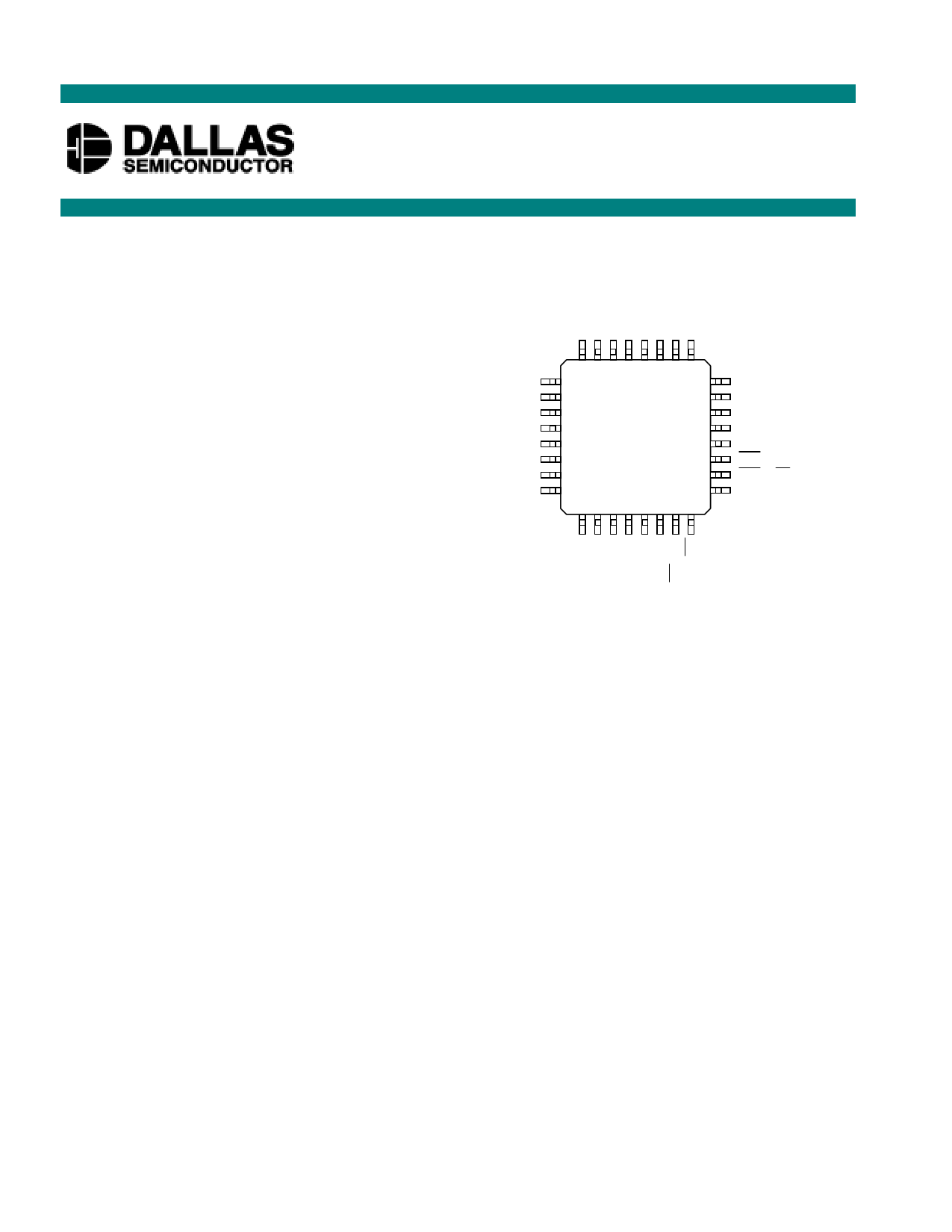
PIN ASSIGNMENT
TL
AD0
AD1
TEST
VSS
AD2
AD3
AD4
32 31 30 29 28 27 26 25
1 24
2 23
3 22
4 DS21372 21
5 32-PIN TQFP 20
6 19
7 18
8 17
9 10 11 12 13 14 15 16
RL
RLOS
LC
VSS
VDD
INT
WR(R/W)
ALE(AS)
ORDERING INFORMATION
DS21372T
(00 C to 700 C)
DS21372TN (-400 C to +850 C)
DESCRIPTION
The DS21372 Bit Error Rate Tester (BERT) is a software programmable test pattern generator, receiver,
and analyzer capable of meeting the most stringent error performance requirements of digital
transmission facilities. Two categories of test pattern generation (Pseudo-random and Repetitive)
conform to CCITT/ITU O.151, O.152, O.153, and O.161 standards. The DS21372 operates at clock rates
ranging from DC to 20 MHz. This wide range of operating frequency allows the DS21372 to be used in
existing and future test equipment, transmission facilities, switching equipment, multiplexers, DACs,
Routers, Bridges, CSUs, DSUs, and CPE equipment.
The DS21372 user-programmable pattern registers provide the unique ability to generate loopback
patterns required for T1, Fractional-T1, Smart Jack, and other test procedures. Hence the DS21372 can
initiate the loopback, run the test, check for errors, and finally deactivate the loopback.
The DS21372 consists of four functional blocks: the pattern generator, pattern detector, error counter, and
control interface. The DS21372 can be programmed to generate any pseudorandom pattern with length up
to 232-1 bits (see Table 5, Note 9) or any user programmable bit pattern from 1 to 32 bits in length. Logic
inputs can be used to configure the DS21372 for applications requiring gap clocking such as Fractional-
T1, Switched-56, DDS, normal framing requirements, and per-channel test procedures. In addition, the
DS21372 can insert single or 10-1 to 10-7 bit errors to verify equipment operation and connectivity.
1 of 21
050400
1 page 
DS21372
PIN SYMBOL TYPE DESCRIPTION
24 RL
25 RDATA
I Receive Load. A positive-going edge loads the previous 32 bits of data
received at RDATA into the Pattern Receive Registers. RL is logically
OR’ed with control bit PCR.3. Should be tied to VSS if not used.
I Receive Data. Received NRZ serial data, sampled on the rising edge of
RCLK.
26 RDIS
I Receive Disable. Set high to prevent the data at RDATA from being
sampled. Set low to allow bits at RDATA to be sampled. Should be tied
to VSS if not used. See Figure 6 for timing information. All receive side
operations are disabled when RDIS is high.
27 RCLK
I Receive Clock. Input clock from transmission link. 0 to 20 MHz. Can
be a gapped clock. Fully independent from TCLK.
28 VDD
29 VSS
30 TCLK
- Positive Supply. 3.3 volts.
- Signal Ground. 0.0 volts. Should be tied to local ground plane.
I Transmit Clock. Transmit demand clock. 0 to 20 MHz. Can be a
gapped clock. Fully independent of RCLK.
31 TDIS
I Transmit Disable. Set high to hold the current bit being transmitted at
TDATA. Set low to allow the next bit to appear at TDATA. Should be
tied to VSS if not used. See Figure 7 for timing information. All transmit
side operations are disabled when TDIS is high.
32 TDATA
O Transmit Data. Transmit NRZ serial data, updated on the rising edge of
TCLK.
DS21372 REGISTER MAP Table 2
ADDRESS R/W REGISTER NAME
00 R/W Pattern Set Register 3.
01 R/W Pattern Set Register 2.
02 R/W Pattern Set Register 1.
03 R/W Pattern Set Register 0.
04 R/W Pattern Length Register.
05 R/W Polynomial Tap Register.
06 R/W Pattern Control Register.
07 R/W Error Insert Register.
08 R Bit Counter Register 3.
09 R Bit Counter Register 2.
0A R Bit Counter Register 1.
0B R Bit Counter Register 0.
ADDRESS
0C
0D
0E
0F
10
11
12
13
14
15
1C
R/W
R
R
R
R
R
R
R
R
R
R/W
R/W
REGISTER NAME
Bit Error Counter Register 3.
Bit Error Counter Register 2.
Bit Error Counter Register 1.
Bit Error Counter Register 0.
Pattern Receive Register 3.
Pattern Receive Register 2.
Pattern Receive Register 1.
Pattern Receive Register 0.
Status Register.
Interrupt Mask Register.
Test Register (see note 1)
NOTE:
1. The Test Register must be set to 00 hex to insure proper operation of the DS21372.
5 of 21
5 Page 
REPETITIVE PATTERN GENERATION (PCR.5=0) Table 5
PATTERN TYPE
PTR PLR PSR3 PSR2 PSR1
all 1s
00 00 FF FF FF
all 0s
00 00 FF FF FF
alternating 1s and 0s
00 01 FF FF FF
double alternating 1s and 0s
00 03 FF FF FF
3 in 24
00 17 FF 20 00
1 in 16
00 0F FF FF 00
1 in 8
00 07 FF FF FF
1 in 4
00 03 FF FF FF
D4 Line Loopback Activate
00 04 FF FF FF
D4 Line Loopback Deactivate
00 02 FF FF FF
PSR0
FF
FE
FE
FC
22
01
01
F1
F0
FC
DS21372
TINV
0
0
0
0
0
0
0
0
0
0
RINV
0
0
0
0
0
0
0
0
0
0
Notes For Tables 4 And 5:
1. PTR = Polynomial Tap Register (address = 05)
2. PLR = Pattern Length Register (address = 04)
3. PSR3 = Pattern Set Register 3 (address = 00)
4. PSR2 = Pattern Set Register 2 (address = 01)
5. PSR1 = Pattern Set Register 1 (address = 02)
6. PSR0 = Pattern Set Register 0 (address = 03)
7. TINV = Transmit Data Inversion Select Bit (EIR.5)
8. RINV = Receive Data Inversion Select Bit (EIR.4)
9. For the 232 -1 pattern, the random pattern actually repeats every (4093 x 220) + 1046529 bits instead of
232 - 1.
8. BIT COUNT REGISTERS
The Bit Count Registers (BCR3 to BCR0) comprise a 32-bit count of bits (actually RCLK cycles)
received at RDATA. BC31 is the MSB of the 32-bit count. The bit counter increments for each cycle of
RCLK when input pin RDIS is low. The bit counter is disabled during loss of SYNC. The Status Register
bit BCOF is set when this 32-bit register overflows. Upon an overflow condition, the user must clear the
BCR by either toggling the LC bit or pin. The DS21372 latches the bit count into the BCR registers and
clears the internal bit count when either the PCR.4 bit or the LC input pin toggles from low to high. The
bit count and bit error count (available via the BECRs) are used by an external processor to compute the
BER performance on a loop or channel basis.
11 of 21
11 Page | ||
| Páginas | Total 21 Páginas | |
| PDF Descargar | [ Datasheet DS21372TN.PDF ] | |
Hoja de datos destacado
| Número de pieza | Descripción | Fabricantes |
| DS21372T | 3.3V Bit Error Rate Tester BERT | Dallas Semiconducotr |
| DS21372TN | 3.3V Bit Error Rate Tester BERT | Dallas Semiconducotr |
| Número de pieza | Descripción | Fabricantes |
| SLA6805M | High Voltage 3 phase Motor Driver IC. |
Sanken |
| SDC1742 | 12- and 14-Bit Hybrid Synchro / Resolver-to-Digital Converters. |
Analog Devices |
|
DataSheet.es es una pagina web que funciona como un repositorio de manuales o hoja de datos de muchos de los productos más populares, |
| DataSheet.es | 2020 | Privacy Policy | Contacto | Buscar |