|
|
|
PDF FDU6692 Data sheet ( Hoja de datos )
| Número de pieza | FDU6692 | |
| Descripción | 30V N-Channel PowerTrench MOSFET | |
| Fabricantes | Fairchild Semiconductor | |
| Logotipo | ||
Hay una vista previa y un enlace de descarga de FDU6692 (archivo pdf) en la parte inferior de esta página. Total 6 Páginas | ||
|
No Preview Available !
April 2001
FDD6692/FDU6692
30V N-Channel PowerTrench MOSFET
General Description
This N-Channel MOSFET has been designed
specifically to improve the overall efficiency of DC/DC
converters using either synchronous or conventional
switching PWM controllers. It has been optimized for
low gate charge, low RDS( ON) and fast switching speed.
Applications
• DC/DC converter
• Motor drives
Features
• 54 A, 30 V.
RDS(ON) = 12 mΩ @ VGS = 10 V
RDS(ON) = 14.5 mΩ @ VGS = 4.5 V
• Low gate charge (18 nC typical)
• Fast switching
• High performance trench technology for extremely
low RDS(ON)
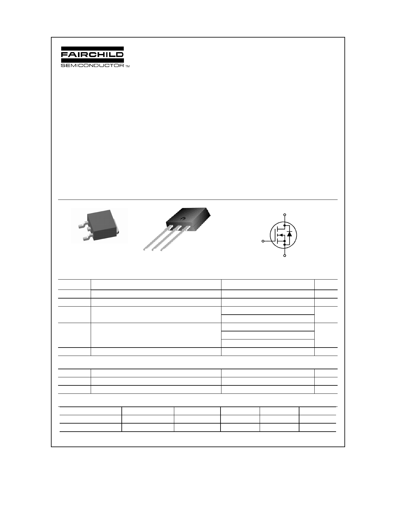
D
G
S
DTO-P-2A5K2
(TO-252)
GDS
I-PAK
(TO-251AA)
D
G
S
Absolute Maximum Ratings TA=25oC unless otherwise noted
Symbol
VDSS
VGSS
ID
PD
Parameter
Drain-Source Voltage
Gate-Source Voltage
Drain Current – Continuous
– Pulsed
Power Dissipation for Single Operation
(Note 3)
(Note 1a)
(Note 1)
(Note 1a)
(Note 1b)
TJ, TSTG
Operating and Storage Junction Temperature Range
Ratings
30
±16
54
162
57
3.8
1.6
-55 to +175
Thermal Characteristics
RθJC Thermal Resistance, Junction-to-Case
RθJA Thermal Resistance, Junction-to-Ambient
RθJA Thermal Resistance, Junction-to-Ambient
(Note 1)
(Note 1a)
(Note 1b)
2.6
40
96
Package Marking and Ordering Information
Device Marking
Device
Package
FDD6692
FDD6692
D-PAK (TO-252)
FDU6692
FDU6692
I-PAK (TO-251)
Reel Size
13’’
Tube
Tape width
12mm
N/A
Units
V
V
A
W
°C
°C/W
°C/W
°C/W
Quantity
2500 units
75
2001 Fairchild Semiconductor Corporation
FDD/FDU6692 Rev C(W)
1 page 
Typical Characteristics
10
ID = 14A
8
6
VDS = 10V
20V
15V
4
2
0
0 5 10 15 20 25 30 35
Qg, GATE CHARGE (nC)
Figure 7. Gate Charge Characteristics.
1000
100
RDS(ON) LIMIT
10
1
VGS = 10V
SINGLE PULSE
0.1 RθJA = 96oC/W
TA = 25oC
100µs
1ms
10ms
100ms
1s
10s
DC
0.01
0.01
0.1 1 10
VDS, DRAIN-SOURCE VOLTAGE (V)
100
Figure 9. Maximum Safe Operating Area.
3000
2500
2000
CISS
f = 1MHz
VGS = 0 V
1500
1000
500
CRSS
0
0
COSS
5 10 15 20 25
VDS, DRAIN TO SOURCE VOLTAGE (V)
30
Figure 8. Capacitance Characteristics.
80
SINGLE PULSE
RθJA = 96°C/W
60 TA = 25°C
40
20
0
0.1
1 10 100
t1, TIME (sec)
1000
Figure 10. Single Pulse Maximum
Power Dissipation.
1
0.1
0.01
D = 0.5
0.2
0.1
0.05
0.02
0.01
0.001
0.001
SINGLE PULSE
0.01
0.1 1 10
t1, TIME (sec)
RθJA(t) = r(t) + RθJA
RθJA = 96 °C/W
P(pk)
t1
t2
TJ - TA = P * RθJA(t)
Duty Cycle, D = t1 / t2
100 1000
Figure 11. Transient Thermal Response Curve.
Thermal characterization performed using the conditions described in Note 1b.
Transient thermal response will change depending on the circuit board design.
FDD/ FDU6692 Rev. C(W)
5 Page | ||
| Páginas | Total 6 Páginas | |
| PDF Descargar | [ Datasheet FDU6692.PDF ] | |
Hoja de datos destacado
| Número de pieza | Descripción | Fabricantes |
| FDU6692 | 30V N-Channel PowerTrench MOSFET | Fairchild Semiconductor |
| FDU6696 | 30V N-Channel PowerTrench MOSFET | Fairchild Semiconductor |
| Número de pieza | Descripción | Fabricantes |
| SLA6805M | High Voltage 3 phase Motor Driver IC. |
Sanken |
| SDC1742 | 12- and 14-Bit Hybrid Synchro / Resolver-to-Digital Converters. |
Analog Devices |
|
DataSheet.es es una pagina web que funciona como un repositorio de manuales o hoja de datos de muchos de los productos más populares, |
| DataSheet.es | 2020 | Privacy Policy | Contacto | Buscar |