|
|
|
PDF FDFS2P106A Data sheet ( Hoja de datos )
| Número de pieza | FDFS2P106A | |
| Descripción | Integrated 60V P-Channel PowerTrench MOSFET and Schottky Diode | |
| Fabricantes | Fairchild Semiconductor | |
| Logotipo | ||
Hay una vista previa y un enlace de descarga de FDFS2P106A (archivo pdf) en la parte inferior de esta página. Total 6 Páginas | ||
|
No Preview Available !
June 2001
FDFS2P106A
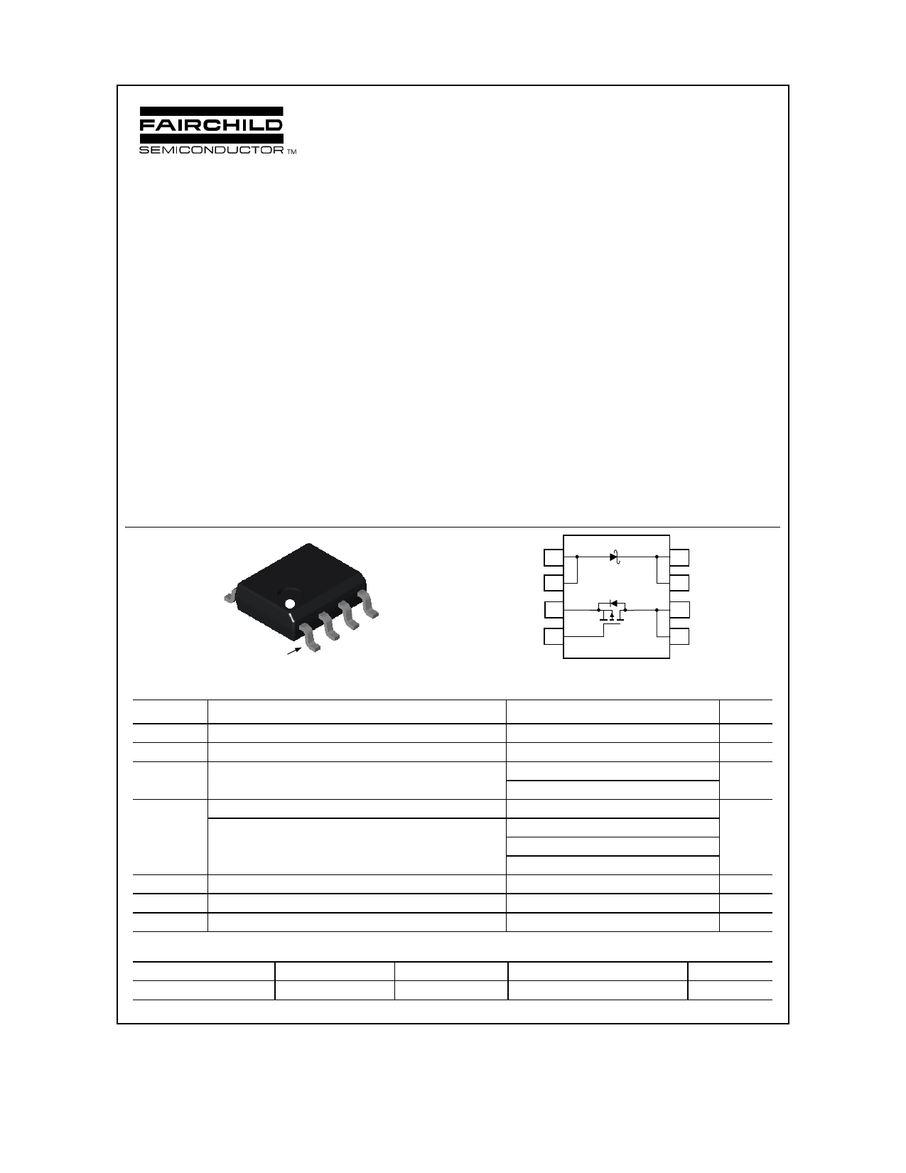
Integrated 60V P-Channel PowerTrench MOSFET and Schottky Diode
General Description
The FDFS2P106A combines the exceptional
performance of Fairchild's PowerTrench MOSFET
technology with a very low forward voltage drop
Schottky barrier rectifier in an SO-8 package.
This device is designed specifically as a single package
solution for DC to DC converters. It features a fast
switching, low gate charge MOSFET with very low on-
state resistance. The independently connected
Schottky diode allows its use in a variety of DC/DC
converter topologies.
Features
• –3.0 A, –60V RDS(ON) = 110 mΩ @ VGS = –10 V
RDS(ON) = 140 mΩ @ VGS = –4.5 V
• VF < 0.45 V @ 1 A (TJ = 125°C)
VF < 0.53 V @ 1 A
VF < 0.62 V @ 2 A
• Schottky and MOSFET incorporated into single
power surface mount SO-8 package
• Electrically independent Schottky and MOSFET
pinout for design flexibility
D
D
C
C
SO-8
Pin 1
G
S
A
A
A1
A2
S3
G4
Absolute Maximum Ratings TA=25oC unless otherwise noted
Symbol
VDSS
VGSS
ID
PD
Parameter
MOSFET Drain-Source Voltage
MOSFET Gate-Source Voltage
Drain Current – Continuous
– Pulsed
Power Dissipation for Dual Operation
Power Dissipation for Single Operation
(Note 1a)
(Note 1a)
(Note 1b)
(Note 1c)
TJ, TSTG
VRRM
IO
Operating and Storage Junction Temperature Range
Schottky Repetitive Peak Reverse Voltage
Schottky Average Forward Current
(Note 1a)
Package Marking and Ordering Information
Device Marking
Device
Reel Size
FDFS2P106A
FDFS2P106A
13’’
Ratings
–60
±20
–3
–10
2
1.6
1
0.9
–55 to +150
45
1
Tape width
12mm
8C
7C
6D
5D
Units
V
V
A
W
°C
V
A
Quantity
2500 units
2001 Fairchild Semiconductor Corporation
FDFS2P106A Rev B(W)
1 page 
Typical Characteristics
10
ID = -3A
8
VDS = -20V
-40V
6
-30V
4
2
0
0 3 6 9 12 15
Qg, GATE CHARGE (nC)
Figure 7. Gate Charge Characteristics.
10
TJ = 125oC
1
0.1
0.01
TJ = 25oC
0.001
0
0.1 0.2 0.3 0.4 0.5 0.6 0.7 0.8
VF, FORWARD VOLTAGE (V)
Figure 9. Schottky Diode Forward Voltage.
1000
800
600
400
200
0
0
CISS
f = 1MHz
VGS = 0 V
COSS
CRSS
5 10 15
-VDS, DRAIN TO SOURCE VOLTAGE (V)
20
Figure 8. Capacitance Characteristics.
1.00E-01
1.00E-02
1.00E-03
1.00E-04
1.00E-05
1.00E-06
1.00E-07
1.00E-08
0
TJ = 125oC
TJ = 25oC
10 20 30 40
VR, REVERSE VOLTAGE (V)
50
60
Figure 10. Schottky Diode Reverse Current.
1
D = 0.5
0.2
0.1 0.1
0.05
0.02
0.01
RθJA(t) = r(t) + RθJA
RθJA = 135 °C/W
P(pk)
t1
t2
TJ - TA = P * RθJA(t)
Duty Cycle, D = t1 / t2
SINGLE PULSE
0.01
0.001
0.01
0.1
1
10 100
Figure 11. Transient Thermal Response Curve.
Thermal characterization performed using the conditions described in Note 1c.
Transient thermal response will change depending on the circuit board design.
1000
FDFS2P106A Rev B(W)
5 Page | ||
| Páginas | Total 6 Páginas | |
| PDF Descargar | [ Datasheet FDFS2P106A.PDF ] | |
Hoja de datos destacado
| Número de pieza | Descripción | Fabricantes |
| FDFS2P106A | Integrated 60V P-Channel PowerTrench MOSFET and Schottky Diode | Fairchild Semiconductor |
| Número de pieza | Descripción | Fabricantes |
| SLA6805M | High Voltage 3 phase Motor Driver IC. |
Sanken |
| SDC1742 | 12- and 14-Bit Hybrid Synchro / Resolver-to-Digital Converters. |
Analog Devices |
|
DataSheet.es es una pagina web que funciona como un repositorio de manuales o hoja de datos de muchos de los productos más populares, |
| DataSheet.es | 2020 | Privacy Policy | Contacto | Buscar |