|
|
|
PDF FB180SA10 Data sheet ( Hoja de datos )
| Número de pieza | FB180SA10 | |
| Descripción | Power MOSFET ( Transistor ) | |
| Fabricantes | International Rectifier | |
| Logotipo | ||
Hay una vista previa y un enlace de descarga de FB180SA10 (archivo pdf) en la parte inferior de esta página. Total 8 Páginas | ||
|
No Preview Available !
l Fully Isolated Package
l Easy to Use and Parallel
l Very Low On-Resistance
l Dynamic dv/dt Rating
l Fully Avalanche Rated
l Simple Drive Requirements
l Low Drain to Case Capacitance
l Low Internal Inductance
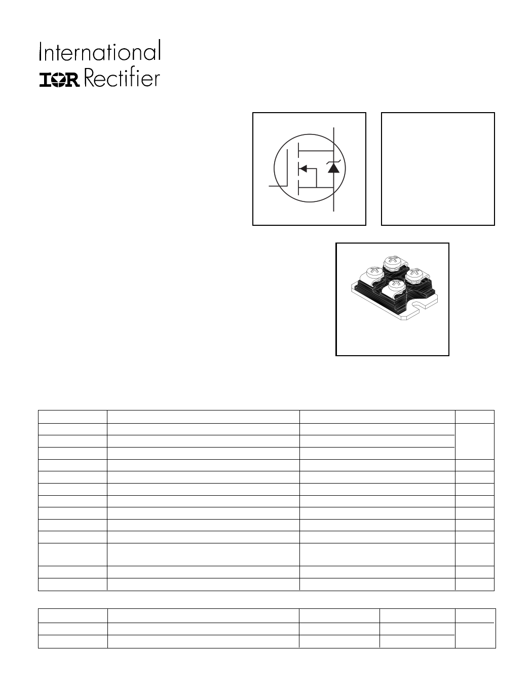
G
Description
Fifth Generation, high current density HEXFETS are
paralled into a compact, high power module providing
the best combination of switching, ruggedized design,
very low ON resistance and cost effectiveness.
The isolated SOT-227 package is preferred for all
commercial - industrial applications at power
dissipation levels to approximately 500 watts. The low
thermal resistance and easy connection to the SOT-
227 package contribute to its universal acceptance
throughout the industry.
Absolute Maximum Ratings
ID @ TC = 25°C
ID @ TC = 100°C
IDM
PD @TC = 25°C
VGS
EAS
IAR
EAR
dv/dt
TJ
TSTG
VISO
Parameter
Continuous Drain Current, VGS @ 10V
Continuous Drain Current, VGS @ 10V
Pulsed Drain Current
Power Dissipation
Linear Derating Factor
Gate-to-Source Voltage
Single Pulse Avalanche Energy
Avalanche Current
Repetitive Avalanche Energy
Peak Diode Recovery dv/dt
Operating Junction and
Storage Temperature Range
Insulation Withstand Voltage (AC-RMS)
Mounting torque, M4 srew
Thermal Resistance
RqJC
RqCS
1
Parameter
Junction-to-Case
Case-to-Sink, Flat, Greased Surface
PD- 91651C
FB180SA10
HEXFET® Power MOSFET
D VDSS = 100V
RDS(on) = 0.0065W
ID = 180A
S
S O T -22 7
Max.
180
120
720
480
2.7
± 20
700
180
48
5.7
-55 to + 150
2.5
1.3
Units
A
W
W/°C
V
mJ
A
mJ
V/ns
°C
kV
N•m
Typ.
–––
0.05
Max.
Units
0.26
––– °C/W
www.irf.com
2/1/99
1 page 
200
175
150
125
100
75
50
25
0
25
50 75 100 125
TC , Case Temperature ( °C)
150
Fig 9. Maximum Drain Current Vs.
Case Temperature
1
FB180SA10
VDS
VGS
RG
RD
D.U.T.
10V
Pulse Width £1 µs
Duty Factor £ 0.1 %
+-VDD
Fig 10a. Switching Time Test Circuit
VDS
90%
10%
VGS
td(on) tr
td(off) tf
Fig 10b. Switching Time Waveforms
D = 0.50
0.1
0.20
0.10
0.05
0.01
0.02
0.01
0.001
0.00001
SINGLE PULSE
(THERMAL RESPONSE)
PDM
t1
t2
Notes:
1. Duty factor D = t1 / t 2
2. Peak TJ = P DM x ZthJC + TC
0.0001
0.001
0.01
t1 , Rectangular Pulse Duration (sec)
Fig 11. Maximum Effective Transient Thermal Impedance, Junction-to-Case
www.irf.com
0.1
5
5 Page | ||
| Páginas | Total 8 Páginas | |
| PDF Descargar | [ Datasheet FB180SA10.PDF ] | |
Hoja de datos destacado
| Número de pieza | Descripción | Fabricantes |
| FB180SA10 | Power MOSFET ( Transistor ) | International Rectifier |
| Número de pieza | Descripción | Fabricantes |
| SLA6805M | High Voltage 3 phase Motor Driver IC. |
Sanken |
| SDC1742 | 12- and 14-Bit Hybrid Synchro / Resolver-to-Digital Converters. |
Analog Devices |
|
DataSheet.es es una pagina web que funciona como un repositorio de manuales o hoja de datos de muchos de los productos más populares, |
| DataSheet.es | 2020 | Privacy Policy | Contacto | Buscar |