|
|
PDF FIN1216MTD Data sheet ( Hoja de datos )
| Número de pieza | FIN1216MTD | |
| Descripción | LVDS 21-Bit Serializers/De-Serializers | |
| Fabricantes | Fairchild Semiconductor | |
| Logotipo | ||
Hay una vista previa y un enlace de descarga de FIN1216MTD (archivo pdf) en la parte inferior de esta página. Total 17 Páginas | ||
|
No Preview Available !
October 2003
Revised October 2004
FIN1217 • FIN1218 •
FIN1215 • FIN1216
LVDS 21-Bit Serializers/De-Serializers
General Description
The FIN1217 and FIN1215 transform 21-bit wide parallel
LVTTL (Low Voltage TTL) data into 3 serial LVDS (Low
Voltage Differential Signaling) data streams. A phase-
locked transmit clock is transmitted in parallel with the data
stream over a separate LVDS link. Every cycle of transmit
clock 21 bits of input LVTTL data are sampled and trans-
mitted.
The FIN1218 and FIN1216 receive and convert the 3 serial
LVDS data streams back into 21 bits of LVTTL data. Refer
to Table 1 for a matrix summary of the Serializers and De-
serializers available. For the FIN1217, at a transmit clock
frequency of 85 MHz, 21 bits of LVTTL data are transmitted
at a rate of 595 Mbps per LVDS channel.
These chipsets are an ideal solution to solve EMI and
cable size problems associated with wide and high-speed
TTL interfaces.
Features
s Low power consumption
s 20 MHz to 85 MHz shift clock support
s 50% duty cycle on the clock output of receiver
s ±1V common-mode range around 1.2V
s Narrow bus reduces cable size and cost
s High throughput (up to 1.785 Gbps throughput)
s Up to 595 Mbps per channel
s Internal PLL with no external component
s Compatible with TIA/EIA-644 specification
s Devices are offered in 48-lead TSSOP packages
Ordering Code:
Order Number Package Number
Package Description
FIN1215MTD
MTD48
48-Lead Thin Shrink Small Outline Package (TSSOP), JEDEC MO-153, 6.1mm Wide
FIN1216MTD
MTD48
48-Lead Thin Shrink Small Outline Package (TSSOP), JEDEC MO-153, 6.1mm Wide
FIN1217MTD
MTD48
48-Lead Thin Shrink Small Outline Package (TSSOP), JEDEC MO-153, 6.1mm Wide
FIN1218MTD
MTD48
48-Lead Thin Shrink Small Outline Package (TSSOP), JEDEC MO-153, 6.1mm Wide
Devices also available in Tape and Reel. Specify by appending suffix letter “X” to the ordering code.
© 2004 Fairchild Semiconductor Corporation DS500876
www.fairchildsemi.com
1 page 
Truth Tables
Transmitter Truth Table
TxIn
Active
Active
F
F
X
H = HIGH Logic Level
L = LOW Logic Level
X = Don’t Care
Z = High Impedance
F = Floating
Inputs
TxCLKIn
Active
L/H/Z
Active
F
X
PwrDn (Note 1)
H
H
H
H
L
TxOut±
L/H
L/H
L
L
Z
Outputs
TxCLKOut±
L/H
X (Note 2)
L/H
X (Note 2)
Z
Note 1: The outputs of the transmitter or receiver will remain in a High Impedance state until VCC reaches 2V.
Note 2: TxCLKOut± will settle at a free running frequency when the part is powered up, PwrDn is HIGH and the TxCLKIn is a steady logic level (L/H/Z).
Receiver Truth Table
RxIn±
Active
Active
F (Note 4)
F (Note 4)
X
H = HIGH Logic Level
L = LOW Logic Level
P = Last Valid State
X = Don’t Care
Z = High Impedance
F = Failsafe Condition
Inputs
RxCLKIn±
Active
F (Note 4)
Active
F (Note 4)
X
PwrDn (Note 3)
H
H
H
H
L
Outputs
RxOut
L/H
P
H
P (Note 5)
L
RxCLKOut
L/H
H
L/H
H
H
Note 3: The outputs of the transmitter or receiver will remain in a High Impedance state until VCC reaches 2V.
Note 4: Failsafe condition is defined as the input being terminated and un-driven (Z) or shorted or open.
Note 5: If RxCLKIn± is removed prior to the RxIn± data being removed, RxOut will be the last valid state. If RxIn± data is removed prior to RxCLKIn± being
removed, RxOut will be HIGH.
5 www.fairchildsemi.com
5 Page 
AC Loading and Waveforms
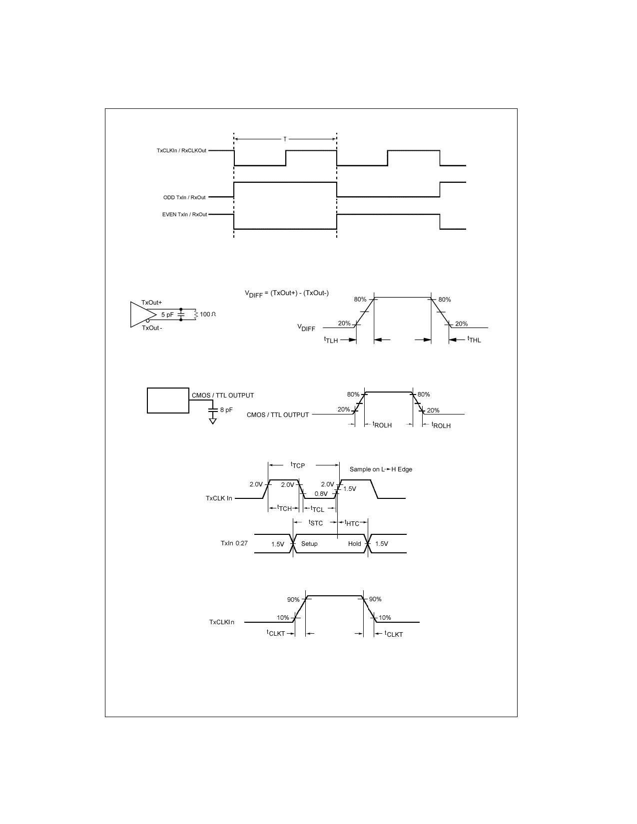
Note: The worst case test pattern produces a maximum toggling of digital circuits, LVDS I/O and LVTTL/CMOS I/O. Depending on the valid strobe edge of
transmitter, the TxCLKIn can be either rising or falling edge data strobe.
FIGURE 3. “Worst Case” Test Pattern
FIGURE 4. Transmitter LVDS Output Load and Transition Times
FIGURE 5. Receiver LVTTL/CMOS Output Load and Transition Times
FIGURE 6. Transmitter Setup/Hold and HIGH/LOW Times (Rising Edge Strobe)
FIGURE 7. Transmitter Input Clock Transition Time
11 www.fairchildsemi.com
11 Page | ||
| Páginas | Total 17 Páginas | |
| PDF Descargar | [ Datasheet FIN1216MTD.PDF ] | |
Hoja de datos destacado
| Número de pieza | Descripción | Fabricantes |
| FIN1216MTD | LVDS 21-Bit Serializers/De-Serializers | Fairchild Semiconductor |
| Número de pieza | Descripción | Fabricantes |
| SLA6805M | High Voltage 3 phase Motor Driver IC. |
Sanken |
| SDC1742 | 12- and 14-Bit Hybrid Synchro / Resolver-to-Digital Converters. |
Analog Devices |
|
DataSheet.es es una pagina web que funciona como un repositorio de manuales o hoja de datos de muchos de los productos más populares, |
| DataSheet.es | 2020 | Privacy Policy | Contacto | Buscar |
