|
|
|
PDF FIN1022MTC Data sheet ( Hoja de datos )
| Número de pieza | FIN1022MTC | |
| Descripción | 2 X 2 LVDS High Speed Crosspoint Switch | |
| Fabricantes | Fairchild Semiconductor | |
| Logotipo | ||
Hay una vista previa y un enlace de descarga de FIN1022MTC (archivo pdf) en la parte inferior de esta página. Total 10 Páginas | ||
|
No Preview Available !
September 2001
Revised December 2001
FIN1022
2 X 2 LVDS High Speed Crosspoint Switch
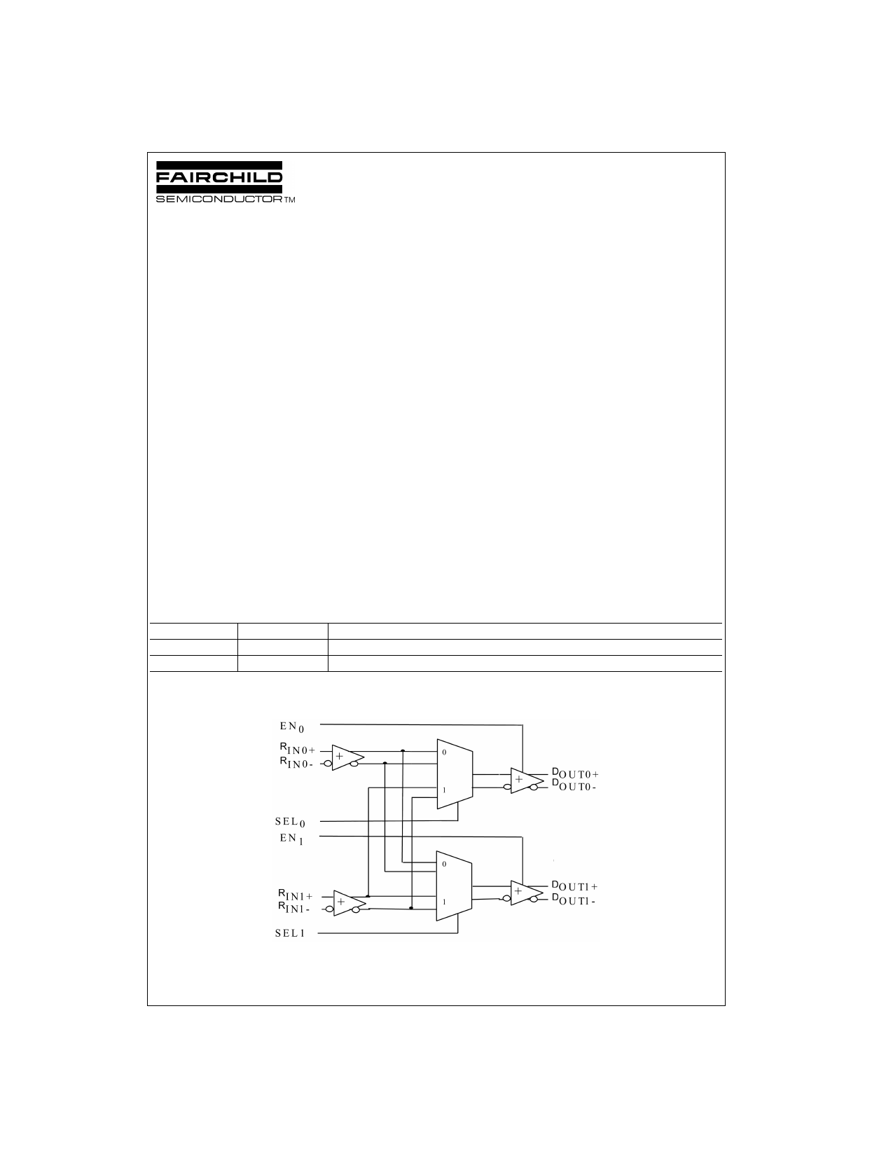
General Description
This non-blocking 2x2 crosspoint switch has a fully differ-
ential input to output data path for low noise generation and
low pulse width distortion. The device can be used as a
high speed crosspoint switch, 2:1 multiplexer, 1:2 demulti-
plexer or 1:2 signal splitter. The inputs can directly interface
with LVDS and LVPECL levels.
Features
s Low jitter, 800 Mbps full differential data path
s Worst case jitter of 190ps
with PRBS = 223 − 1 data pattern at 800 Mbps
s Rail-to-rail common mode range is 0.5V to 3.25V
s Worst case power dissipation is less than 126 mW
s Open-circuit fail safe protection
s Fast switch time of 1.1 ns typical
s 35 ps typical pin channel to channel skew
s 3.3V power supply operation
s Non-blocking switch
s LVDS receiver inputs accept LVPECL signals directly
s 7.5 kV HBM ESD protection
s 16-lead SOIC package and TSSOP package
s Inter-operates with TIA/EIA 644-1995 specification
s See the Fairchild Interface Solutions web page for cross
reference information:
www.fairchildsemi.com/products/interface/lvds.html
Ordering Code:
Order Number Package Number
Package Description
FIN1022M
M16A
16-Lead Small Outline Integrated Circuit (SOIC), JEDEC MS-012, 0.150" Narrow
FIN1022MTC
MTC16
16-Lead Thin Shrink Small Outline Package (TSSOP), JEDEC MO-153, 4.4mm Wide
Devices also available in Tape and Reel. Specify by appending suffix letter “X” to the ordering code.
Logic Symbol
© 2001 Fairchild Semiconductor Corporation DS500653
www.fairchildsemi.com
1 page 
Required Specifications
1. When the true and complement LVDS outputs (having
a 75Ω connected between outputs) are connected to
3.75 kΩ resistors and the common point of those 3.75
kΩ resistors are connected to a voltage source that
sweeps from 0 to 2.4V, the DC VOD and ∆VOD are still
maintained (see Figure 1).
2. When the true and complement LVDS outputs (having
a 5 pF capacitor attached between outputs) are con-
nected with 37.5Ω resistors each to common point,
then the common point does not vary by more than 150
mV under all process, temperature and voltage condi-
tions when the outputs switch either from LOW-to-
HIGH or from HIGH-to-LOW (see Figure 2).
3. Pull-down resistors are required on Enable (EN0 and
EN1) and select (SEL0 and SEL1) inputs.
4. Fail safe protection on the outputs that draw less than
20 µA of current (worst case) on the LVDS inputs. In
this condition, if the input is in fail safe selected to
OUT0+/OUT0− (say) and the outputs are Enabled then
OUT0+ = HIGH and OUT0− = LOW. This prevents noise
from being amplified when the connection is broken.
5. In the disabled state the outputs can go beyond VCC
but there should be no appreciable leakage (see IOZD
and IOFF specifications)
FIGURE 1. Common Mode Supply Test Circuit
FIGURE 2. Dynamic VOS Test Circuit and Waveforms
5 www.fairchildsemi.com
5 Page | ||
| Páginas | Total 10 Páginas | |
| PDF Descargar | [ Datasheet FIN1022MTC.PDF ] | |
Hoja de datos destacado
| Número de pieza | Descripción | Fabricantes |
| FIN1022MTC | 2 X 2 LVDS High Speed Crosspoint Switch | Fairchild Semiconductor |
| Número de pieza | Descripción | Fabricantes |
| SLA6805M | High Voltage 3 phase Motor Driver IC. |
Sanken |
| SDC1742 | 12- and 14-Bit Hybrid Synchro / Resolver-to-Digital Converters. |
Analog Devices |
|
DataSheet.es es una pagina web que funciona como un repositorio de manuales o hoja de datos de muchos de los productos más populares, |
| DataSheet.es | 2020 | Privacy Policy | Contacto | Buscar |