|
|
|
PDF M2086 Data sheet ( Hoja de datos )
| Número de pieza | M2086 | |
| Descripción | VCSO FEC PLL WITH AUTOSWITCH FOR SONET/OTN | |
| Fabricantes | Integrated Circuit Solution Inc | |
| Logotipo | ||
Hay una vista previa y un enlace de descarga de M2086 (archivo pdf) en la parte inferior de esta página. Total 14 Páginas | ||
|
No Preview Available !
Integrated
Circuit
Systems, Inc.
P r e l i m i n a r y I n f o r m a t i o n M2080/81/82
M2085/86/87
VCSO FEC PLL WITH AUTOSWITCH FOR SONET/OTN
GENERAL DESCRIPTION
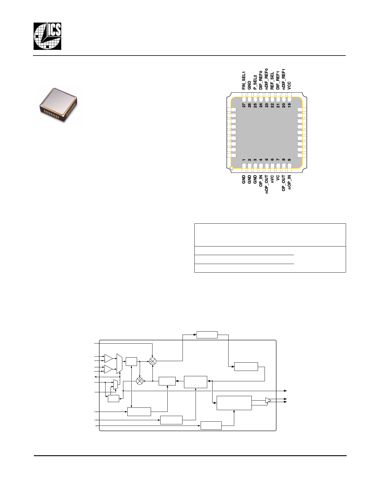
PIN ASSIGNMENT (9 x 9 mm SMT)
The M2080/81/82 and M2085/86/87 are VCSO (Voltage
Controlled SAW Oscillator) based
clock PLLs designed for FEC clock
ratio translation in 10Gb optical
systems such as OC-192 or 10GbE.
They support FEC (Forward Error
Correction) clock multiplication
ratios, both forward (mapping) and
inverse (de-mapping). Multiplication ratios are
pin-selected from pre-programming look-up tables.
FEATURES
◆ Integrated SAW delay line; Output of 15 to 700 MHz *
◆ Low phase jitter < 0.5 ps rms typical
(12kHz to 20MHz or 50kHz to 80MHz)
◆ LVPECL clock output (CML and LVDS options available)
◆ Pin-selectable PLL divider ratios support FEC ratios
• M2080/85: OTU1 (255/238) and OTU2 (255/237) Mapping
• M2081/86: OTU1 (238/255) or OTU2 (237/255) De-mapping
• M2082/87: OTU1 (238/255) and OTU2 (237/255) De-mapping
◆ Reference clock inputs support differential LVDS,
LVPECL, as well as single-ended LVCMOS, LVTTL
◆ Loss of Lock (LOL) output pin; Narrow Bandwidth
control input (NBW pin)
◆ AutoSwitch (AUTO pin) - automatic (non-revertive)
reference clock reselection upon clock failure
◆ Acknowledge pin (REF_ACK pin) indicates the actively
selected reference input
◆ Options for Hitless Switching (HS) with or without
Phase Build-out (PBO) to enable SONET (GR-253) /SDH
(G.813) MTIE and TDEV compliance during reselection
◆ Single 3.3V power supply
◆ Small 9 x 9 mm SMT (surface mount) package
FIN_SEL0
FEC_SEL0
FEC_SEL1
LOL
NBW
VCC
DNC
DNC
DNC
28 18
29 17
30 M 2 0 8 0
31
32 S e r i e s
16
15
14
33 13
34 ( T o p V i e w ) 12
35 11
36 10
P_SEL0
P_SEL1
nFOUT
FOUT
GND
REF_ACK
AUTO
VCC
GND
Figure 1: Pin Assignment
Example I/O Clock Frequency Combinations
Using M2081-11-622.0800 FEC De-Map Ratios
FEC De-Map
PLL Ratio
Mfec / Rfec
Base Input Rate 1
(MHz)
Output Clock
(either output)
MHz
1/1
237/255
238/255
622.0800
666.5143
669.3266
622.08
or
155.52
Table 1: Example I/O Clock Frequency Combinations
Note 1: Input reference clock can be the base frequency shown
divided by “Mfin” (as shown in Tables 3 and 4 on pg. 3).
* Specify VCSO center frequency at time of order.
SIMPLIFIED BLOCK DIAGRAM
NBW
DIF_REF0
nDIF_REF0
DIF_REF1
nDIF_REF1
REF_ACK
REF_SEL
AUTO
M2080 Series
MUX
0 Rfec
Div
1
PLL
Phase
Detector
0
1
Auto
Ref Sel
LOL Phase
Detector
Mfec Div
2
FEC_SEL1:0
2
FIN_SEL1:0
3
P_SEL2:0
Mfec / Rfec Divider
LUT
Mfin Divider
LUT
Loop Filter
Mfin Divider
(1, 4, 8, 32 or
1, 4, 8, 16)
VCSO
P Divider
(1, 4, 8, 32 or TriState)
Tri-state
P Divider
LUT
Figure 2: Simplified Block Diagram
LOL
FOUT
nFOUT
M2080/81/82 M2085/86/87 Datasheet Rev 0.4
Revised 30Jul2004
M2080/81/82 VCSO FEC PLL with AutoSwitch for SONET/OTN
Integrated Circuit Systems, Inc. ● Networking & Communications ● www.icst.com ● tel (508) 852-5400
1 page 
Integrated
Circuit
Systems, Inc.
M2080/81/82, M2085/86/87
VCSO FEC PLL WITH AUTOSWITCH FOR SONET/OTN
Preliminary Information
The M208x Series includes a Loss of Lock (LOL)
indicator, which provides status information to system
management software. A Narrow Bandwidth (NBW)
control pin is provided as an additional mechanism for
adjusting PLL loop bandwidth without affecting the
phase detector frequency.
Options are available for Hitless Switching (HS) with or
without Phase Build-out (PBO). They provide SONET/
SDH MTIE and TDEV compliance during a reference
clock reselection.
Input Reference Clocks
Two clock reference inputs and a selection mux are
provided. Either reference clock input can accept a
differential clock signal (such as LVPECL or LVDS) or
a single-ended clock input (LVCMOS or LVTTL on the
non-inverting input).
Differential Inputs
Differential LVPECL inputs are connected to both
reference input pins in the usual manner. The external
load termination resistors shown in Figure 4 (the 127Ω
and 82Ω resistors) is ideally suited for both AC and DC
coupled LVPECL reference clock lines. These provide
the 50Ω load termination and the VTT bias voltage.
Single-ended Inputs
Single-ended inputs (LVCMOS or LVTTL) are
connected to the non-inverting reference input pin
(DIF_REF0 or DIF_REF1). The inverting reference input pin
(nDIF_REF0 or nDIF_REF1) must be left unconnected.
In single-ended operation, when the unused inverting
input pin (nDIF_REF0 or nDEF_REF1) is left floating (not
connected), the input will self-bias at VCC/2.
A single-ended reference clock on the unselected
reference input can cause an increase in output
clock jitter. For this reason, differential reference
inputs are preferred; interference from a differential
input on the non-selected input is minimal.
Configuration of a single-ended input has been
facilitated by biasing nDIF_REF0 and nDEF_REF1 to Vcc/2,
with 50kΩ to Vcc and 50kΩ to ground. The input clock
structure, and how it is used with either
LVCMOS/LVTTL inputs or a DC- coupled LVPECL
clock, is shown in Figure 4.
.
LVCMOS/
LVTTL
DIF_REF0
nDIF_REF0
X
VCC
DIF_REF1 127Ω
LVPECL
VCC
82Ω
127 Ω
nDIF_REF1
82 Ω
REF_SEL
VCC
50kΩ
50kΩ
50kΩ
VCC
50kΩ
50kΩ
50kΩ
Figure 4: Input Reference Clocks
MUX
0
1
PLL Operation
The M2080/81/82 and M2085/86/87 are complete clock
PLLs. They use a phase detector and configurable
dividers to synchronize the output of the VCSO with the
selected reference clock.
The M208x Series components are similar to the
M2060 Series components except that the M208x
Series includes the selectable AutoSwitch feature. The
M208x Series also has only one clock output, as the
AutoSwitch control pins replace of the second output.
The PLL will work correctly, meaning it will phase-lock
the VCSO output to the input reference clock, when the
internal phase detector inputs are able to run at the
same frequency. This means the PLL dividers must be
set appropriately and a suitable reference frequency
must be chosen for the intended output frequency.
When the PLL is not set up appropriately, the VCSO is
forced to its upper or lower operating limit which is typi-
cally about 200 ppm above or below the VCSO center
frequency. See “APR, VCSO Absolute Pull-Range” row,
in the AC Characteristics table on pg. 12.
In normal phase-locked condition, the instantaneous
phase error is measured by the phase detector and is
converted to charge pump current pulses. These
current pulses are then integrated by the external loop
filter to create a VCSO control voltage. The loop filter
acts as a low pass filter to remove unwanted reference
clock jitter above a determined frequency or PLL
bandwidth. For reference phase jitter frequencies within
the loop bandwidth, phase jitter amplitude is passed on
to the output clock according to the PLL loop frequency
response curve.
M2080/81/82 Datasheet Rev 0.4
5 of 14
Revised 30Jul2004
Integrated Circuit Systems, Inc. ● Networking & Communications ● www.icst.com ● tel (508) 852-5400
5 Page 
Integrated
Circuit
Systems, Inc.
M2080/81/82, M2085/86/87
VCSO FEC PLL WITH AUTOSWITCH FOR SONET/OTN
Preliminary Information
ELECTRICAL SPECIFICATIONS
DC Characteristics
Unless stated otherwise, VCC = 3.3V +5%,TA = 0 oC to +70 oC (commercial), TA = -40 oC to +85 oC (industrial), FVCSO = FOUT = 622-675MHz,
LVPECL outputs terminated with 50Ω to VCC - 2V
Symbol Parameter
Min Typ Max Unit Conditions
Power Supply VCC Positive Supply Voltage
3.135 3.3 3.465 V
ICC Power Supply Current
175 225 mA
All
Differential
Inputs
VP-P
VCMR
CIN
Peak to Peak Input Voltage
Common Mode Input
Input Capacitance
DIF_REF0, nDIF_REF0,
DIF_REF1, nDIF_REF1
0.15
0.5
V
Vcc - .85 V
4 pF
Differential
Inputs with
Pull-down
IIH Input High Current (Pull-down)
IIL Input Low Current (Pull-down) DIF_REF0, DIF_REF1
Rpulldown Internal Pull-down Resistance
150 µA
VCC = VIN =
-5 µA 3.456V
50 kΩ
Differential
Inputs
Biased to
VCC/2 1
IIH
IIL
Rbias
Input High Current (Biased) 1
Input Low Current (Biased) 1
Biased to Vcc/2 1
nDIF_REF0, nDIF_REF1
150 µA
-150 µA
(Note 1)
kΩ
VIN =
0 to 3.456V
All LVCMOS
/ LVTTL
Inputs
VIH
VIL
CIN
Input High Voltage
Input Low Voltage
Input Capacitance
AUTO, REF_SEL, FIN_SEL1,
FIN_SEL0, FEC_SEL1,
FEC_SEL0, P_SEL2, P_SEL1,
P_SEL0, NBW
2
-0.3
Vcc + 0.3 V
0.8 V
4 pF
LVCMOS /
LVTTL
Inputs with
Pull-down
IIH Input High Current (Pull-down) AUTO, REF_SEL, FIN_SEL1,
FIN_SEL0, FEC_SEL1,
IIL Input Low Current (Pull-down) FEC_SEL0, P_SEL2, P_SEL1,
Rpulldown Internal Pull-down Resistance P_SEL0
-5
150 µA
µA
VCC = VIN =
3.456V
50 kΩ
LVCMOS /
LVTTL
Inputs with
Pull-UP
IIH
IIL
Rpullup
Input High Current (Pull-UP)
Input Low Current (Pull-UP)
Internal Pull-UP Resistance
NBW
-150
50
5 µA
µA
VCC = 3.456V
VIN = 0 V
kΩ
Differential
Output
LVCMOS
Outputs
VOH
VOL
VP-P
VOH
VOL
Output High Voltage
Output Low Voltage
FOUT, nFOUT
Peak to Peak Output Voltage 2
Output High Voltage
Output Low Voltage
LOL, REF_ACK
Vcc - 1.4
Vcc - 2.0
0.4
2.4
GND
Vcc - 1.0 V
Vcc - 1.7 V
0.85 V
VCC V
0.4 V
IOH= 1mA
IOL= 1mA
Note 1: Biased to Vcc/2, with 50kΩ to Vcc and 50kΩ to ground. See Figure 4, Input Reference Clocks, on pg. 5 Table 14: DC Characteristics
Note 2: Single-ended measurement. See Figure 6, Output Rise and Fall Time, on pg. 12.
M2080/81/82 Datasheet Rev 0.4
11 of 14
Revised 30Jul2004
Integrated Circuit Systems, Inc. ● Networking & Communications ● www.icst.com ● tel (508) 852-5400
11 Page | ||
| Páginas | Total 14 Páginas | |
| PDF Descargar | [ Datasheet M2086.PDF ] | |
Hoja de datos destacado
| Número de pieza | Descripción | Fabricantes |
| M208 | Single Chip Organ | STMicroelectronics |
| M208-A4 | Contact Image Sensor Module | CMOS Sensor |
| M208-A6 | Contact Image Sensor Module | CMOS Sensor |
| M208-A8 | Contact Image Sensor Module | CMOS Sensor |
| Número de pieza | Descripción | Fabricantes |
| SLA6805M | High Voltage 3 phase Motor Driver IC. |
Sanken |
| SDC1742 | 12- and 14-Bit Hybrid Synchro / Resolver-to-Digital Converters. |
Analog Devices |
|
DataSheet.es es una pagina web que funciona como un repositorio de manuales o hoja de datos de muchos de los productos más populares, |
| DataSheet.es | 2020 | Privacy Policy | Contacto | Buscar |