|
|
|
PDF M2021 Data sheet ( Hoja de datos )
| Número de pieza | M2021 | |
| Descripción | VCSO BASED CLOCK PLL | |
| Fabricantes | Integrated Circuit Systems | |
| Logotipo | ||
Hay una vista previa y un enlace de descarga de M2021 (archivo pdf) en la parte inferior de esta página. Total 10 Páginas | ||
|
No Preview Available !
Integrated
Circuit
Systems, Inc.
Product Data Sheet
M2020/21
VCSO BASED CLOCK PLL
GENERAL DESCRIPTION
The M2020/21 is a VCSO (Voltage Controlled SAW
Oscillator) based clock jitter
attenuator PLL designed for clock
jitter attenuation and frequency
translation. The device is ideal for
generating the transmit reference
clock for optical network systems
supporting 2.5-10 GB data rates.
It can serve to jitter attenuate a
stratum reference clock or a recovered clock in loop
timing mode. The M2020/21 module includes a
proprietary SAW (surface acoustic wave) delay line as
part of the VCSO. This results in a high frequency,
high-Q, low phase noise oscillator that assures low
intrinsic output jitter.
FEATURES
◆ Integrated SAW (surface acoustic wave) delay line;
low phase jitter of < 0.5ps rms, typical (12kHz to 20MHz
or 50kHz to 80MHz)
◆ Output frequencies of 15 to 700 MHz *
◆ LVPECL clock output (CML and LVDS options available)
◆ Reference clock inputs support differential LVDS,
LVPECL, as well as single-ended LVCMOS, LVTTL
◆ Loss of Lock (LOL) output pin
◆ Narrow Bandwidth control input (NBW pin)
◆ Hitless Switching (HS) options with or without Phase
Build-out (PBO) available for SONET (GR-253) /
SDH (G.813) MTIE and TDEV compliance during
reference clock reselection
◆ Industrial temperature grade available
◆ Single 3.3V power supply
◆ Small 9 x 9 mm SMT (surface mount) package
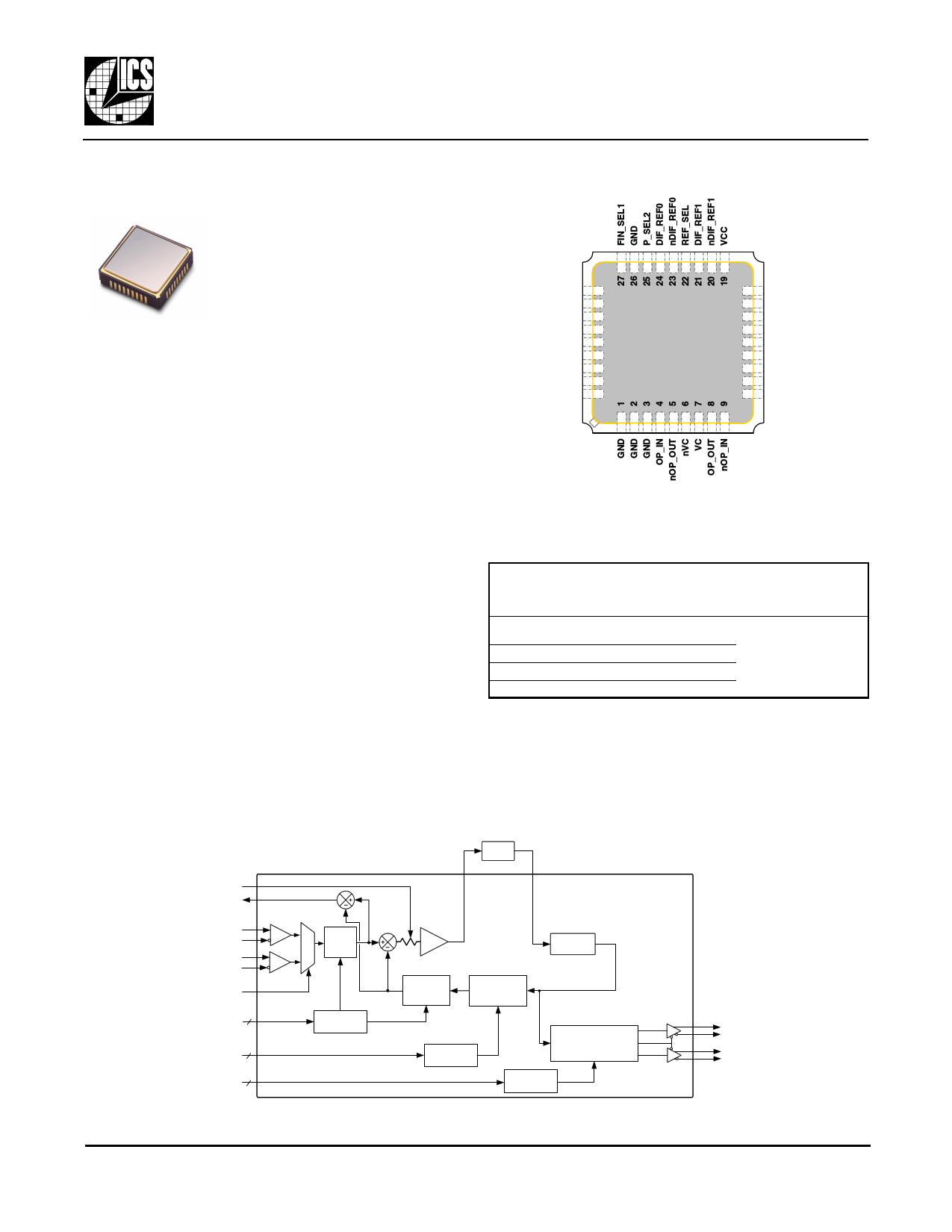
PIN ASSIGNMENT (9 x 9 mm SMT)
FIN_SEL0
MR_SEL0
MR_SEL1
LOL
NBW
VCC
DNC
DNC
DNC
28 18
29 17
30
31
M2020
32 M 2 0 2 1
16
15
14
33
34 ( T o p V i e w )
13
12
35 11
36 10
P_SEL0
P_SEL1
nFOUT0
FOUT0
GND
nFOUT1
FOUT1
VCC
GND
Figure 1: Pin Assignment
Example I/O Clock Frequency Combinations
Using M2020-11-622.0800 or M2021-11-622.0800
Input Reference
Clock (MHz)
PLL Ratio
(Pin Selectable)
Output Clock
(MHz)
(M2020)
(M2021)
19.44 or 38.88
(M2020) (M2021)
32 or 16
77.76
155.52
8 622.08
4
622.08
1
Table 1: Example I/O Clock Frequency Combinations
* Specify VCSO center frequency at time of order.
SIMPLIFIED BLOCK DIAGRAM
NBW
LOL
M2020/21
Loop
Filter
DIF_REF0
nDIF_REF0
DIF_REF1
nDIF_REF1
REF_SEL
MR_SEL1:0 2
FIN_SEL1:0 2
P_SEL2:0 3
MUX
0 R Div
(1, 4,
16, 64)
1
Phase
Detector
VCSO
M / R Divider
LUT
M Divider
(1, 4, 16, 64)
Mfin Div
(1, 4, 8, 32) or
( 1, 4, 8, 16)
Mfin Divider
LUT
P Divider
TriState
FOUT0: 1, 4, 8, 32 or TriState
FOUT1: 1, 4, 8 or TriState
P Divider
LUT
FOUT0
nFOUT0
FOUT1
nFOUT1
Figure 2: Simplified Block Diagram
M2020/21 Datasheet Rev 1.0
Revised 30Jul2004
M2020/21 VCSO Based Clock PLL
Integrated Circuit Systems, Inc. ● Networking & Communications ● www.icst.com ● tel (508) 852-5400
1 page 
Integrated
Circuit
Systems, Inc.
In normal phase-locked condition, the instantaneous
phase error is measured by the phase detector and is
converted to charge pump current pulses. These
current pulses are then integrated by the external loop
filter to create a VCSO control voltage. The loop filter
acts as a low pass filter to remove unwanted reference
clock jitter above a determined frequency or PLL
bandwidth. For reference phase jitter frequencies within
the loop bandwidth, phase jitter amplitude is passed on
to the output clock according to the PLL loop frequency
response curve.
The relationship between the nominal VCSO center
frequency (Fvcso), the M divider, and the input
reference frequency (Fin) is:
Fvcso
=
Fin
× Mfin
×
M---
R
Example Frequency and Divider Combinations
Using M2021-yz-622.0800
Fvcso = Fin x
Mfin x M/R
622.08
38.88
77.76
155.52
622.08
16 x (1/1, 4/4, etc.)
8 x (1/1, 4/4, etc.)
4 x (1/1, 4/4, etc.)
1 x (1/1, 4/4, etc.)
Table 6: Example I/O Clock Frequency Combinations
The M, R, and Mfin dividers can be set by pin configura-
tion using the input pins MR_SEL1, MR_SEL0, FIN_SEL1, and
FIN_SEL0.
Post-PLL Divider
The M2020/21 also features a post-PLL (P) divider.
Through use of the P divider, the device’s output
frequency (Fout) can be that of the VCSO (such as
622.08MHz) or the VCSO frequency divided by 4, 8 or 32
(common optical reference clocks in SONET and SDH
systems).
The P_SEL2:0 pins select the value for the P divider. (See
Table 5 on pg. 3.)
Accounting for the P divider, the complete relationship
between the input clock reference frequency (Fin) and
output clock frequency (Fout) is defined as:
Fout
=
--F----v---c---s---o----
P
=
Fin ×
--M------×-----M-----f--i--n---
R× P
Due to the narrow tuning range of the VCSO (+120ppm
guaranteed), appropriate selection of all of the following
are required for the PLL be able to lock: VCSO center
frequency, input frequency, and divider selections.
M2020/21
VCSO BASED CLOCK PLL
Product Data Sheet
TriState
The TriState feature puts the LVPECL output driver into
a high impedance state, effectively disconnecting the
driver from the FOUT and nFOUT pins of the device. A
logic 0 is then present on the clock net. The impedance
of the clock net is then set to 50Ω by the external circuit
resistors. (This is in distinction to a CMOS output in
TriState, in which case the net goes to a high
impedance and the logic value floats.) The 50Ω
impedance level of the LVPECL TriState allows
manufacturing In-circuit Test to drive the clock net with
an external 50Ω generator to validate the integrity of
clock net and the clock load.
Any unused output (single-ended or differential) should
be left unconnected (floating) in system application.
This minimizes output switching current and therefore
minimizes noise modulation of the VCSO.
Narrow Bandwidth (NBW) Control Pin
A Narrow Loop Bandwidth control pin (NBW pin) is
included to enable adjustment of the PLL loop
bandwidth. In wide bandwidth mode (NBW=0), the
internal resistor Rin is 100kΩ. With the NBW pin
asserted (NBW=1), the internal resistor Rin is changed to
2100kΩ. This lowers the loop bandwidth by a factor of
about 21 (2100 / 100) and lowers the damping factor by
about 4.6 (the square root of 21), assuming the same
external loop filter component values.
Loss of Lock Indicator (LOL) Output Pin
Under normal device operation, when the PLL is locked,
the LOL Phase Detector drives LOL to logic 0. Under
circumstances when the VCSO cannot fully phase lock
to the input (as measured by a greater than 4 ns
discrepancy between the feedback and reference clock
rising edges at the LOL Phase Detector) the LOL output
goes to logic 1. The LOL pin will return back to logic 0
when the phase detector error is less than 2 ns. The
loss of lock indicator is a low current LVCMOS output.
Guidelines for Using LOL
In a given application, the magnitude of peak-to-peak
jitter at the phase detector will usually increase as the R
divider is increased. If the LOL pin will be used to detect
an unusual clock condition, or a clock fault, the
MR_SEL1:0 pins should be set to provide a phase detector
frequency of 5MHz or greater (the phase detector
frequency is equal to Fin divided by the R divider).
Otherwise, false LOL indications may result. A phase
detector frequency of 10MHz or greater is desirable
when reference jitter is over 500ps, or when the device is
used within a noisy system environment. LOL should not
be used when the device is used in a loop timing
application.
M2020/21 Datasheet Rev 1.0
5 of 10
Revised 30Jul2004
Integrated Circuit Systems, Inc. ● Networking & Communications ● www.icst.com ● tel (508) 852-5400
5 Page | ||
| Páginas | Total 10 Páginas | |
| PDF Descargar | [ Datasheet M2021.PDF ] | |
Hoja de datos destacado
| Número de pieza | Descripción | Fabricantes |
| M2020 | VCSO BASED CLOCK PLL | Integrated Circuit Systems |
| M2020-2021 | VCSO BASED CLOCK PLL | Integrated Circuit Systems |
| M2021 | VCSO BASED CLOCK PLL | Integrated Circuit Systems |
| M202xxx | Subminiature / Multi-Function | NKK Switches |
| Número de pieza | Descripción | Fabricantes |
| SLA6805M | High Voltage 3 phase Motor Driver IC. |
Sanken |
| SDC1742 | 12- and 14-Bit Hybrid Synchro / Resolver-to-Digital Converters. |
Analog Devices |
|
DataSheet.es es una pagina web que funciona como un repositorio de manuales o hoja de datos de muchos de los productos más populares, |
| DataSheet.es | 2020 | Privacy Policy | Contacto | Buscar |