|
|
|
PDF LZ2313H5 Data sheet ( Hoja de datos )
| Número de pieza | LZ2313H5 | |
| Descripción | 1/3-type CCD Area Sensors with 270 k Pixels | |
| Fabricantes | Sharp Electrionic Components | |
| Logotipo | ||
Hay una vista previa y un enlace de descarga de LZ2313H5 (archivo pdf) en la parte inferior de esta página. Total 12 Páginas | ||
|
No Preview Available !
LZ2313H5/LZ2314HJ
LZ2313H5/
LZ2314HJ
1/3-type CCD Area Sensors
with 270 k Pixels
DESCRIPTION
The LZ2313H5/LZ2314HJ are 1/3-type (6.0 mm)
solid-state image sensors that consist of PN photo-
diodes and CCDs (charge-coupled devices). With
approximately 270 000 pixels (542 horizontal x 492
vertical), the sensor provides a stable high-resolution
color (LZ2313H5)/B/W (LZ2314HJ) image.
FEATURES
• Number of effective pixels : 512 (H) x 492 (V)
• Number of optical black pixels
– Horizontal : 2 front and 28 rear
• Pixel pitch : 9.6 µm (H) x 7.5 µm (V)
• Mg, G, Cy, and Ye complementary color filters
(For LZ2313H5)
• Low fixed-pattern noise and lag
• No burn-in and no image distortion
• Blooming suppression structure
• Built-in output amplifier
• Variable electronic shutter (1/60 to 1/10 000 s)
• Compatible with NTSC standard (LZ2313H5)/
EIA standard (LZ2314HJ)
• Package :
16-pin shrink-pitch WDIP [Ceramic]
(WDIP016-N-0500C)
Row space : 12.70 mm
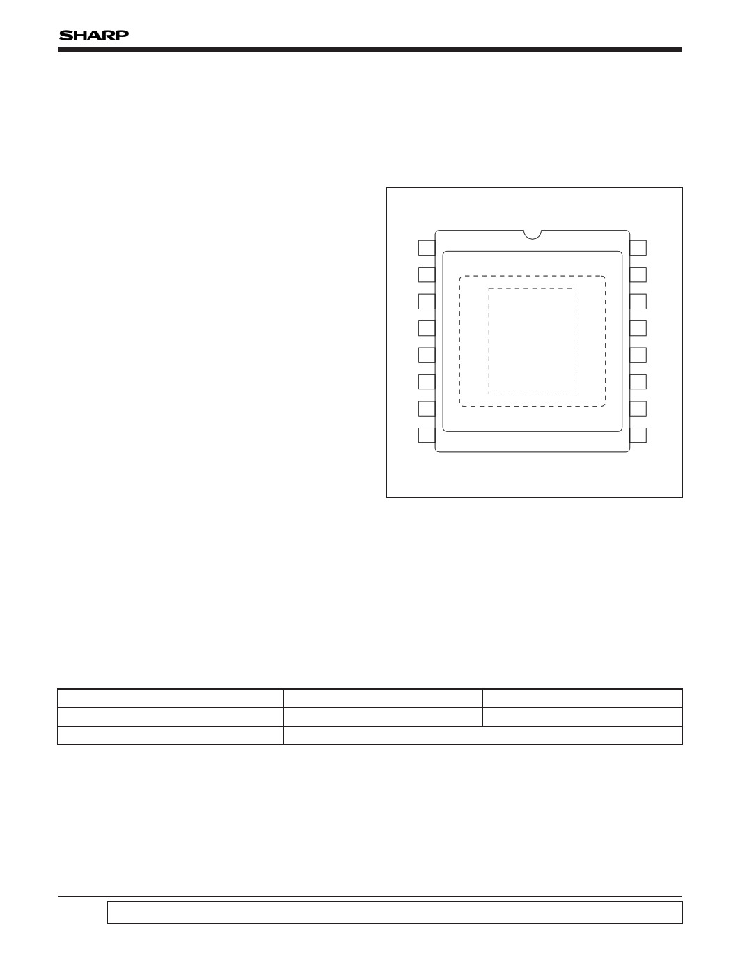
PIN CONNECTIONS
16-PIN SHRINK-PITCH WDIP
TOP VIEW
OD 1
ØRS 2
RD 3
OS 4
NC1 5
NC2 6
ØH2 7
ØH1 8
16 GND
15 ØV4
14 ØV3
13 ØV2
12 ØV1
11 PW
10 OFD
9 T1
(WDIP016-N-0500C)
PRECAUTIONS
• The exit pupil position of lens should be more
than 25 mm (LZ2313H5)/20 mm (LZ2314HJ)
from the top surface of the CCD.
• Refer to "PRECAUTIONS FOR CCD AREA
SENSORS" for details.
COMPARISON TABLE
TV standard
Characteristics
LZ2313H5
LZ2314HJ
NTSC standard (Color)
EIA standard (B/W)
Refer to each following specification.
In the absence of confirmation by device specification sheets, SHARP takes no responsibility for any defects that may occur in equipment using any SHARP devices shown in
catalogs, data books, etc. Contact SHARP in order to obtain the latest device specification sheets before using any SHARP device.
1
1 page 
LZ2313H5/LZ2314HJ
CHARACTERISTICS FOR LZ2314HJ (Drive method : Field accumulation)
(TA = +25 ˚C, Operating conditions : The typical values specified in "RECOMMENDED OPERATING CONDITIONS".
Color temperature of light source : 3 200 K, IR cut-off filter (CM-500, 1 mmt) is used.)
PARAMETER
SYMBOL
MIN. TYP. MAX. UNIT NOTE
Standard output voltage
VO 150 mV 2
Photo response non-uniformity
PRNU
10 %
3
Saturation output voltage
VSAT
700
mV 4
Dark output voltage
VDARK
0.3 3.0 mV 1, 5
Dark signal non-uniformity
DSNU
0.6 2.0 mV 1, 6
Sensitivity
R
560 800
mV 7
Smear ratio
SMR
–90 –76 dB
8
Image lag
AI
1.0 %
9
Blooming suppression ratio
ABL 100
10
Output transistor drain current
IOD 4.0 8.0 mA
Output impedance
RO 350 $
NOTES :
• VOFD should be adjusted to the minimum voltage such
that ABL satisfy the specification, or to the value
displayed on the device.
1. TA = +60 ˚C
2. The average output voltage under uniform illumination.
The standard exposure conditions are defined as when
Vo is 150 mV.
3. The image area is divided into 10 x 10 segments under
the standard exposure conditions. Each segment's
voltage is the average output voltage of all pixels within
the segment. PRNU is defined by (Vmax – Vmin)/Vo,
where Vmax and Vmin are the maximum and minimum
values of each segment's voltage respectively.
4. The image area is divided into 10 x 10 segments. Each
segment's voltage is the average output voltage of all
pixels within the segment. VSAT is the minimum
segment's voltage under 10 times exposure of the
standard exposure conditions.
5. The average output voltage under non-exposure
conditions.
6. The image area is divided into 10 x 10 segments under
non-exposure conditions. DSNU is defined by (Vdmax –
Vdmin), where Vdmax and Vdmin are the maximum and
minimum values of each segment's voltage respectively.
7. The average output voltage when a 1 000 lux light
source with a 90% reflector is imaged by a lens of F4,
f50 mm.
8. The sensor is exposed only in the central area of V/10
square with a lens at F4, where V is the vertical image
size. SMR is defined by the ratio of the output voltage
detected during the vertical blanking period to the
maximum output voltage in the V/10 square.
9. The sensor is exposed at the exposure level
corresponding to the standard conditions. AI is defined
by the ratio of the output voltage measured at the 1st
field during the non-exposure period to the standard
output voltage.
10. The sensor is exposed only in the central area of V/10
square, where V is the vertical image size. ABL is
defined by the ratio of the exposure at the standard
conditions to the exposure at a point where blooming is
observed.
5
5 Page 
PRECAUTIONS FOR CCD AREA SENSORS
1. Package Breakage
In order to prevent the package from being broken,
observe the following instructions :
1) The CCD is a precise optical component and
the package material is ceramic or plastic.
Therefore,
ø Take care not to drop the device when
mounting, handling, or transporting.
ø Avoid giving a shock to the package.
Especially when leads are fixed to the socket
or the circuit board, small shock could break
the package more easily than when the
package isn’t fixed.
2) When applying force for mounting the device or
any other purposes, fix the leads between a
joint and a stand-off, so that no stress will be
given to the jointed part of the lead. In addition,
when applying force, do it at a point below the
stand-off part.
(In the case of ceramic packages)
– The leads of the package are fixed with low
melting point glass, so stress added to a
lead could cause a crack in the low melting
point glass in the jointed part of the lead.
Low melting point glass
Lead
Fixed
Stand-off
PRECAUTIONS FOR CCD AREA SENSORS
(In the case of plastic packages)
– The leads of the package are fixed with
package body (plastic), so stress added to a
lead could cause a crack in the package
body (plastic) in the jointed part of the lead.
Glass cap
Package
Lead
Fixed
Stand-off
3) When mounting the package on the housing,
be sure that the package is not bent.
– If a bent package is forced into place
between a hard plate or the like, the pack-
age may be broken.
4) If any damage or breakage occurs on the sur-
face of the glass cap, its characteristics could
deteriorate.
Therefore,
ø Do not hit the glass cap.
ø Do not give a shock large enough to cause
distortion.
ø Do not scrub or scratch the glass surface.
– Even a soft cloth or applicator, if dry, could
cause dust to scratch the glass.
2. Electrostatic Damage
As compared with general MOS-LSI, CCD has
lower ESD. Therefore, take the following anti-static
measures when handling the CCD :
1) Always discharge static electricity by grounding
the human body and the instrument to be used.
To ground the human body, provide resistance
of about 1 M$ between the human body and
the ground to be on the safe side.
2) When directly handling the device with the
fingers, hold the part without leads and do not
touch any lead.
11
11 Page | ||
| Páginas | Total 12 Páginas | |
| PDF Descargar | [ Datasheet LZ2313H5.PDF ] | |
Hoja de datos destacado
| Número de pieza | Descripción | Fabricantes |
| LZ2313H5 | 1/3-type CCD Area Sensors with 270 k Pixels | Sharp Electrionic Components |
| Número de pieza | Descripción | Fabricantes |
| SLA6805M | High Voltage 3 phase Motor Driver IC. |
Sanken |
| SDC1742 | 12- and 14-Bit Hybrid Synchro / Resolver-to-Digital Converters. |
Analog Devices |
|
DataSheet.es es una pagina web que funciona como un repositorio de manuales o hoja de datos de muchos de los productos más populares, |
| DataSheet.es | 2020 | Privacy Policy | Contacto | Buscar |