|
|
|
PDF DAC7615EB Data sheet ( Hoja de datos )
| Número de pieza | DAC7615EB | |
| Descripción | Quad/ Serial Input/ 12-Bit/ Voltage Output DIGITAL-TO-ANALOG CONVERTER | |
| Fabricantes | Burr-Brown Corporation | |
| Logotipo | ||
Hay una vista previa y un enlace de descarga de DAC7615EB (archivo pdf) en la parte inferior de esta página. Total 12 Páginas | ||
|
No Preview Available !
® DAC7615
DAC7615
DAC7615
Quad, Serial Input, 12-Bit, Voltage Output
DIGITAL-TO-ANALOG CONVERTER
FEATURES
q LOW POWER: 20mW
q UNIPOLAR OR BIPOLAR OPERATION
q SETTLING TIME: 10µs to 0.012%
q 12-BIT LINEARITY AND MONOTONICITY:
–40°C to +85°C
q DOUBLE-BUFFERED DATA INPUTS
q SMALL 20-LEAD SSOP PACKAGE
APPLICATIONS
q PROCESS CONTROL
q ATE PIN ELECTRONICS
q CLOSED-LOOP SERVO-CONTROL
q MOTOR CONTROL
q DATA ACQUISITION SYSTEMS
q DAC-PER-PIN PROGRAMMERS
DESCRIPTION
The DAC7615 is a quad, serial input, 12-bit, voltage
output digital-to-analog converter (DAC) with guar-
anteed 12-bit monotonic performance over the –40°C
to +85°C temperature range. An asynchronous reset
clears all registers to either mid-scale (800H) or zero-
scale (000H), selectable via the RESETSEL pin. The
individual DAC inputs are double buffered to allow
GND
for simultaneous update of all DAC outputs. The
device can be powered from a single +5V supply or
from dual +5V and –5V supplies.
Low power and small size makes the DAC7615 ideal
for automatic test equipment, DAC-per-pin program-
mers, data acquisition systems, and closed-loop servo-
control. The device is available in 16-pin plastic DIP,
16-lead SOIC, and 20-lead SSOP packages and is
guaranteed over the –40°C to +85°C temperature range.
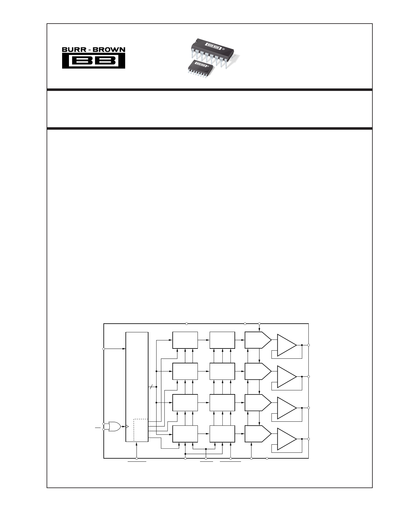
VDD VREFH
Input
DAC
Register A
Register A
DAC A
VOUTA
SDI
CLK
CS
Serial-to-
Parallel
Shift
Register
12
Input
Register B
DAC
Register B
DAC B
Input
Register C
DAC
Register C
DAC C
DAC
Select
Input
Register D
DAC
Register D
DAC D
VOUTB
VOUTC
VOUTD
LOADREG
RESETSEL RESET LOADDACS VREFL VSS
International Airport Industrial Park • Mailing Address: PO Box 11400, Tucson, AZ 85734 • Street Address: 6730 S. Tucson Blvd., Tucson, AZ 85706 • Tel: (520) 746-1111 • Twx: 910-952-1111
Internet: http://www.burr-brown.com/ • FAXLine: (800) 548-6133 (US/Canada Only) • Cable: BBRCORP • Telex: 066-6491 • FAX: (520) 889-1510 • Immediate Product Info: (800) 548-6132
© 1998 Burr-Brown Corporation
PDS-1443C
Printed in U.S.A. November, 1998
1 page 
TYPICAL PERFORMANCE CURVES: VSS = 0V
At TA = +25°C, VDD = +5V, VSS = 0V, VREFH = +2.5V, and VREFL = 0V, representative unit, unless otherwise specified.
0.50
LINEARITY ERROR and
DIFFERENTIAL LINEARITY ERROR vs CODE
(DAC A)
0.25
0.00
–0.25
–0.50
0.50
0.25
0.00
–0.25
–0.50
000H
200H
400H
600H 800H A00H
Digital Input Code
C00H
E00H
FFFH
LINEARITY ERROR and
DIFFERENTIAL LINEARITY ERROR vs CODE
(DAC B)
0.50
0.25
0.00
–0.25
–0.50
0.50
0.25
0.00
–0.25
–0.50
000H
200H
400H
600H 800H A00H
Digital Input Code
C00H
E00H
FFFH
0.50
LINEARITY ERROR and
DIFFERENTIAL LINEARITY ERROR vs CODE
(DAC C)
0.25
0.00
–0.25
–0.50
0.50
0.25
0.00
–0.25
–0.50
000H
200H
400H
600H 800H A00H
Digital Input Code
C00H
E00H
FFFH
0.50
LINEARITY ERROR and DIFFERENTIAL
LINEARITY ERROR vs CODE
(DAC D)
0.25
0.00
–0.25
–0.50
0.50
0.25
0.00
–0.25
–0.50
000H
200H
400H
600H 800H A00H
Digital Input Code
C00H
E00H
FFFH
0.50
+85°C
0.25
LINEARITY ERROR vs CODE
(DAC A, –40°C and +85°C)
0.00
–0.25
–0.50
0.50
–40°C
0.25
0.00
–0.25
–0.50
000H
200H
400H
600H 800H A00H
Digital Input Code
C00H
E00H
FFFH
0.50
+85°C
0.25
LINEARITY ERROR vs CODE
(DAC B, –40°C and +85°C)
0.00
–0.25
–0.50
0.50
–40°C
0.25
0.00
–0.25
–0.50
000H
200H
400H
600H 800H A00H
Digital Input Code
C00H
E00H
FFFH
®
5 DAC7615
5 Page 
STATE OF
SELECTED
SELECTED
STATE OF
INPUT
INPUT
ALL DAC
A1
A0
LOADREG LOADDACS
RESET
REGISTER
REGISTER
REGISTERS
L(1) L L H(2) H
L HL H H
H LL H H
H HL H H
X(3) X H L H
X XH H H
X XX X L
A
B
C
D
NONE
NONE
ALL
Transparent
Transparent
Transparent
Transparent
(All Latched)
(All Latched)
Reset(4)
Latched
Latched
Latched
Latched
Transparent
Latched
Reset(4)
NOTES: (1) L = Logic LOW. (2) H = Logic HIGH. (3) X = Don’t Care. (4) Resets to either 000H or 800H, per the RESETSEL state (LOW = 000H, HIGH = 800H).
When RESET rises, all registers that are in their latched state retain the reset value.
TABLE II. Control Logic Truth Table.
CS(1) CLK(1) LOADREG RESET SERIAL SHIFT REGISTER
H(2)
X(3)
L(4) L
L ↑(5)
↑L
H(6) X
H(6) X
H
H
H
H
L(7)
H
H
H
H
H
H
L(8)
No Change
No Change
Advanced One Bit
Advanced One Bit
No Change
No Change
NOTES: (1) CS and CLK are interchangeable. (2) H = Logic HIGH. (3) X =
Don’t Care. (4) L = Logic LOW (5) = Positive Logic Transition. (6) A HIGH
value is suggested in order to avoid a “false clock” from advancing the shift
register and changing the shift register. (7) If data is clocked into the serial
register while LOADREG is LOW, the selected input register will change as the
shift register bits “flow” through A1 and A0. This will corrupt the data in each
input register that has been erroneously selected. (8) RESET LOW causes no
change in the contents of the serial shift register.
TABLE III. Serial Shift Register Truth Table.
Note that CS and CLK are combined with an OR gate and
the output controls the serial-to-parallel shift register inter-
nal to the DAC7615 (see the block diagram on the front of
this data sheet). These two inputs are completely inter-
changeable. In addition, care must be taken with the state of
CLK when CS rises at the end of a serial transfer. If CLK is
LOW when CS rises, the OR gate will provide a rising edge
to the shift register, shifting the internal data one additional
bit. The result will be incorrect data and possible selection of
the wrong input register.
If both CS and CLK are used, then CS should rise only when
CLK is HIGH. If not, then either CS or CLK can be used to
operate the shift register. See Table III for more information.
The digital data into the DAC7615 is double-buffered. This
allows new data to be entered for each DAC without disturb-
ing the analog outputs. When the new settings have been
entered into the device, all of the DAC outputs can be
updated simultaneously. The transfer from the input regis-
ters to the DAC registers is accomplished with a HIGH to
LOW transition on the LOADDACS input.
Because the DAC registers become transparent when
LOADDACS is LOW, it is possible to keep this pin LOW
and update each DAC via LOADREG. However, as each
new data word is entered into the device, the corresponding
output will update immediately when LOADREG is taken
LOW.
Digital Input Coding
The DAC7615 input data is in Straight Binary format. The
output voltage is given by the following equation:
VOUT
=
VREFL
+
(VREFH
– VREFL)
4096
•
N
where N is the digital input code (in decimal). This equation
does not include the effects of offset (zero-scale) or gain
(full-scale) errors.
®
11 DAC7615
11 Page | ||
| Páginas | Total 12 Páginas | |
| PDF Descargar | [ Datasheet DAC7615EB.PDF ] | |
Hoja de datos destacado
| Número de pieza | Descripción | Fabricantes |
| DAC7615E | Quad/ Serial Input/ 12-Bit/ Voltage Output DIGITAL-TO-ANALOG CONVERTER | Burr-Brown Corporation |
| DAC7615EB | Quad/ Serial Input/ 12-Bit/ Voltage Output DIGITAL-TO-ANALOG CONVERTER | Burr-Brown Corporation |
| Número de pieza | Descripción | Fabricantes |
| SLA6805M | High Voltage 3 phase Motor Driver IC. |
Sanken |
| SDC1742 | 12- and 14-Bit Hybrid Synchro / Resolver-to-Digital Converters. |
Analog Devices |
|
DataSheet.es es una pagina web que funciona como un repositorio de manuales o hoja de datos de muchos de los productos más populares, |
| DataSheet.es | 2020 | Privacy Policy | Contacto | Buscar |