|
|
|
PDF DAC707JP Data sheet ( Hoja de datos )
| Número de pieza | DAC707JP | |
| Descripción | Microprocessor-Compatible 16-BIT DIGITAL-TO-ANALOG CONVERTERS | |
| Fabricantes | Burr-Brown Corporation | |
| Logotipo | ||
Hay una vista previa y un enlace de descarga de DAC707JP (archivo pdf) en la parte inferior de esta página. Total 11 Páginas | ||
|
No Preview Available !
DAC707
® DAC708
DAC709
Microprocessor-Compatible
16-BIT DIGITAL-TO-ANALOG CONVERTERS
FEATURES
q TWO-CHIP CONSTRUCTION
q HIGH-SPEED 16-BIT PARALLEL, 8-BIT
(BYTE) PARALLEL, AND SERIAL INPUT
MODES
q DOUBLE-BUFFERED INPUT REGISTER
CONFIGURATION
q VOUT AND IOUT MODELS
DESCRIPTION
The DAC708 and DAC709 are 16-bit converters de-
signed to interface to an 8-bit microprocessor bus. 16-
bit data is loaded in two successive 8-bit bytes into
parallel 8-bit latches before being transferred into the
D/A latch. The DAC708 and DAC709 are current and
voltage output models respectively and are in 24-pin
hermetic DIPs. Input coding is Binary Two’s Comple-
ment (bipolar) or Unipolar Straight Binary (unipolar,
when an external logic inverter is used to invert the
MSB). In addition, the DAC708/709 can be loaded
serially (MSB first).
The DAC707 is designed to interface to a 16-bit bus.
q HIGH ACCURACY:
Linearity Error ±0.003% of FSR max
Differential Linearity Error ±0.006% of FSR
max
q MONOTONIC (TO 14 BITS) OVER
SPECIFIED TEMPERATURE RANGE
q HERMETICALLY SEALED
q LOW COST PLASTIC VERSIONS
AVAILABLE (DAC707JP/KP)
Data is written into a 16-bit latch and subsequently the
D/A latch. The DAC707 has bipolar voltage output
and input coding is Binary Two’s Complement (BTC).
All models have Write and Clear control lines as well
as input latch enable lines. In addition, DAC708 and
DAC709 have Chip Select control lines. In the bipolar
mode, the Clear input sets the D/A latch to give zero
voltage or current output. They are all 14-bit accurate
and are complete with reference, and for the DAC707,
and DAC709, a voltage output amplifier. All models
are available with an optional burn-in screening.
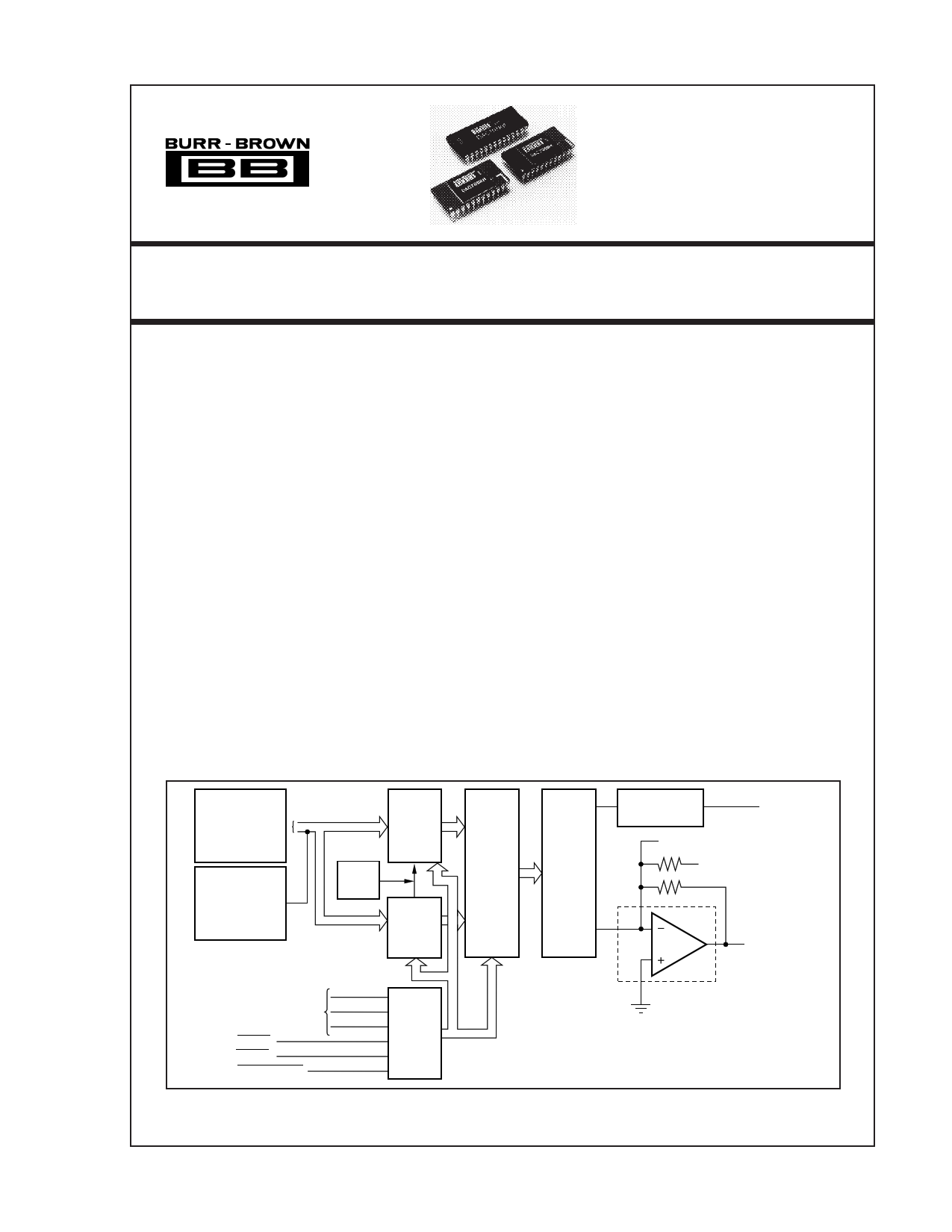
8-Bit
(DAC708, 709)
or
16-Bit (DAC707)
Serial
(DAC708, 709)
Serial
Data
High
Byte
Latch
Low
Byte
Latch
D/A
Latch
16-Bit
D/A
Con-
verter
Reference
Circuit
Bipolar
Offset
Summing Junction (708, 709)
10V Range (708, 709)
VOUT
Latch Enables/
Mode Select
CLEAR
WRITE
CHIP SELECT
Control
Logic
DAC707 or DAC709
Only
DAC707/708/709 Block Diagram
International Airport Industrial Park • Mailing Address: PO Box 11400, Tucson, AZ 85734 • Street Address: 6730 S. Tucson Blvd., Tucson, AZ 85706 • Tel: (520) 746-1111 • Twx: 910-952-1111
Internet: http://www.burr-brown.com/ • FAXLine: (800) 548-6133 (US/Canada Only) • Cable: BBRCORP • Telex: 066-6491 • FAX: (520) 889-1510 • Immediate Product Info: (800) 548-6132
PDS-557H
1 page 
DESCRIPTION OF PIN FUNCTIONS
DAC707
DESIGNATOR
DESCRIPTION
VOUT
VDD
Voltage output for DAC707 (±10V)
Logic supply (+5V)
Pin
# DESIGNATOR
1 A2
2 A0
DCOM
Digital common
3 A1
ACOM
SJ
GA
+VCC
–VCC
CLR
WR
A1
A0
D15 (MSB)
Analog common
4 D7 (D15)
Summing junction of the internal output op amp for the 5 D6 (D14)
DAC707. Offset adjust circuit is connected to the
summing junction of the output amplifier. Refer to Block
Diagram.
Gain adjust pin. Refer to Connection Diagram for gain
adjust circuit.
6 D5 (D13)
Positive supply voltage (+15V)
7 D4 (D12)
Negative supply voltage (–15V)
8 D3 (D11)
Clear line. Sets the input latch to zero and sets the D/A 9 D2 (D10)
latch to the input code that gives bipolar zero on the
D/A output (Active low)
Write control line (Active low)
10 D1 (D9)
Enable for D/A converter latch (Active low)
11 D0 (D8)/SI
Enable for input latch (Active low)
Data bit 15 (Most Significant Bit)
12 DCOM
13 RF2
D14 Data bit 14
14 VOUT
RF1 (DAC708)
D13 Data bit 13
D12 Data bit 12
15 ACOM
16 SJ (DAC709)
IOUT (DAC708)
D11 Data bit 11
D10 Data bit 10
D9 Data bit 9
D8 Data bit 8
D7 Data bit 7
17 BPO
18 GA
19 +VCC
20 –VCC
21 CLR
D6
D5
D4
D3
D2
D1
D0 (LSB)
Data bit 6
Data bit 5
Data bit 4
Data bit 3
Data bit 2
Data bit 1
Data bit 0 (Least Significant Bit)
22 WR
23 CS
24 VDD
25 No pin
26 No pin
27 No pin
28 No pin
DAC708/709
DESCRIPTION
Latch enable for D/A latch (Active low)
Latch enable for “low byte” input (Active low). When
both A0 and A1 are logic “0”, the serial input mode is
selected and the serial input is enabled.
Latch enable for “high byte” input (Active low). When
both A0 and A1 are logic “0”, the serial input mode is
selected and the serial input is enabled.
Input for data bit 7 if enabling low byte (LB) latch or
data bit 15 if enabling the high byte (HB) latch.
Input for data bit 6 if enabling LB latch or data bit 14 if
enabling the HB latch.
Data bit 5 (LB) or data bit 13 (HB)
Data bit 4 (LB) or data bit 12 (HB)
Data bit 3 (LB) or data bit 11 (HB)
Data bit 2 (LB) or data bit 10 (HB)
Data bit 1 (LB) or data bit 9 (HB)
Data bit 0 (LB) or data bit 8 (HB). Serial input when
serial mode is selected.
Digital common
Feedback resistor for internal or external operational
amplifier. Connect to pin 14 when a 10V output range
is desired. Leave open for a 20V output range.
Voltage output for DAC709 or feedback resistor for
use with an external output op amp for the DAC708.
Refer to Connection Diagram for connection of
external op amp to DAC708.
Analog common
Summing junction of the internal output op amp for the
DAC709, or the current output for the DAC708. Refer
to Connection Diagram for connection of external op
amp to DAC708.
Bipolar offset. Connect to pin 16 when operating in the
bipolar mode. Leave open for unipolar mode.
Gain adjust pin
Positive supply voltage (+15V)
Negative supply voltage (–15V)
Clear line. Sets the high and low byte input registers
to zero and, for bipolar operation, sets the D/A register
to the input code that gives bipolar zero on the D/A
output. (In the unipolar mode, invert the MSB prior to
the D/A.)
Write control line
Chip select control line
Logic supply (+5V)
(The DAC708 and DAC709 are in 24-pin packages)
®
5 DAC707/708/709
5 Page 
74LS161A Synchronous Binary Counter
VDD Carry Out
ENT QA
ENP QB
0.001µF 2.2kΩ
Load QC No
QD Connection
A
+5V
CLR
In
B
C
CK D
1/4 74LS00
VDD
330Ω
DATA STROBE
1/6 7407
VDD
330Ω
Serial Input
(16-Bit Data
Stream) 1/6 7407
VDD
330Ω
VDD
2.2kΩ
TIL117
VDD
2.2kΩ
A2 A1 A0 CS
Analog
WR
Output
CLR
DAC708
or
DAC709
DO
1/4 74LS00
1/4 74LS00
VDD
2.2kΩ
+
10k Ω
+
+
RESET
1/6 7407
+
VDD 2.2µF
+
Power
Supply
Voltage
–
Isolated
Power
Supply
DATA STROBE
Serial Input
A2
Isolation Barrier
...
13
24
..1. 4 15 16
Analog
Output
FIGURE 10. Serial Loading of Electrically Isolated DAC708/709.
WR
D16
16-Bit Data Bus
D0
µP
A15
16-Bit
Address
Bus
A1
A0
Base
Address
Decoder
CS1
CS2
FIGURE 11. Connecting Multiple DAC707s to a 16-Bit Microprocessor.
11
A0 WR VOUT1
DAC707
A1
A0 WR VOUT2
DAC707
A1
DAC707/708/709
®
11 Page | ||
| Páginas | Total 11 Páginas | |
| PDF Descargar | [ Datasheet DAC707JP.PDF ] | |
Hoja de datos destacado
| Número de pieza | Descripción | Fabricantes |
| DAC707JP | Microprocessor-Compatible 16-BIT DIGITAL-TO-ANALOG CONVERTERS | Burr-Brown Corporation |
| Número de pieza | Descripción | Fabricantes |
| SLA6805M | High Voltage 3 phase Motor Driver IC. |
Sanken |
| SDC1742 | 12- and 14-Bit Hybrid Synchro / Resolver-to-Digital Converters. |
Analog Devices |
|
DataSheet.es es una pagina web que funciona como un repositorio de manuales o hoja de datos de muchos de los productos más populares, |
| DataSheet.es | 2020 | Privacy Policy | Contacto | Buscar |