|
|
|
PDF 100311 Data sheet ( Hoja de datos )
| Número de pieza | 100311 | |
| Descripción | Low Skew 1:9 Differential Clock Driver | |
| Fabricantes | Fairchild Semiconductor | |
| Logotipo | ||
Hay una vista previa y un enlace de descarga de 100311 (archivo pdf) en la parte inferior de esta página. Total 6 Páginas | ||
|
No Preview Available !
February 1990
Revised November 1999
100311
Low Skew 1:9 Differential Clock Driver
General Description
The 100311 contains nine low skew differential drivers,
designed for generation of multiple, minimum skew differ-
ential clocks from a single differential input (CLKIN,
CLKIN). If a single-ended input is desired, the VBB output
pin may be used to drive the remaining input line. A HIGH
on the enable pin (EN) will force a LOW on all of the CLKn
outputs and a HIGH on all of the CLKn output pins. The
100311 is ideal for distributing a signal throughout a system
without worrying about the original signal becoming too
corrupted by undesirable delays and skew.
Features
s Low output-to-output skew
s 2000V ESD protection
s 1:9 low skew clock driver
s Differential inputs and outputs
s Available to industrial grade temperature range
(PLCC package only)
Ordering Code:
Order Number Package Number
Package Description
100311QC
V28A
28-Lead Plastic Lead Chip Carrier (PLCC), JEDEC MO-047, 0.450 Square
100311QI
V28A
28-Lead Plastic Lead Chip Carrier (PLCC), JEDEC MO-047, 0.450 Square
Industrial Temperature Range (−40°C to +85°C)
Devices also available in Tape and Reel. Specify by appending the suffix letter “X” to the ordering code.
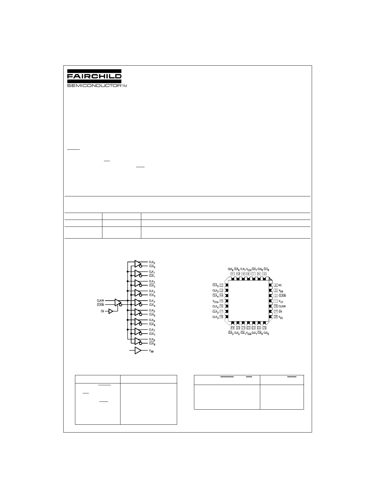
Logic Symbol
Connection Diagram
28-Pin PLCC
Pin Descriptions
Pin Names
CLKIN, CLKIN
EN
CLK0–8, CLK0–8
VBB
NC
Description
Differential Clock Inputs
Enable
Differential Clock Outputs
VBB Output
No Connect
Truth Table
CLKIN
L
H
X
CLKIN
H
L
X
EN
L
L
H
CLKn
L
H
L
CLKn
H
L
H
© 1999 Fairchild Semiconductor Corporation DS010648
www.fairchildsemi.com
1 page 
Test Circuit
Note:
Shown for testing CLKIN to CLK1 in the differential mode.
L1, L2, L3 and L4 = equal length 50Ω impedance lines.
All unused inputs and outputs are loaded with 50Ω in parallel with ≤ 3 pF to GND.
Scope should have 50Ω input terminator internally.
FIGURE 1. AC Test Circuit
Switching Waveforms
FIGURE 2. Propagation Delay, EN to Outputs
FIGURE 3. Propagation Delay, CLKIN/CLKIN to Outputs
FIGURE 4. Transition Times
5
www.fairchildsemi.com
5 Page | ||
| Páginas | Total 6 Páginas | |
| PDF Descargar | [ Datasheet 100311.PDF ] | |
Hoja de datos destacado
| Número de pieza | Descripción | Fabricantes |
| 100310 | Low Skew 2:8 Differential Clock Driver | Fairchild Semiconductor |
| 100310QC | Low Skew 2:8 Differential Clock Driver | Fairchild Semiconductor |
| 100310QI | Low Skew 2:8 Differential Clock Driver | Fairchild Semiconductor |
| 100311 | Low Skew 1:9 Differential Clock Driver | Fairchild Semiconductor |
| Número de pieza | Descripción | Fabricantes |
| SLA6805M | High Voltage 3 phase Motor Driver IC. |
Sanken |
| SDC1742 | 12- and 14-Bit Hybrid Synchro / Resolver-to-Digital Converters. |
Analog Devices |
|
DataSheet.es es una pagina web que funciona como un repositorio de manuales o hoja de datos de muchos de los productos más populares, |
| DataSheet.es | 2020 | Privacy Policy | Contacto | Buscar |