|
|
|
PDF DAN222 Data sheet ( Hoja de datos )
| Número de pieza | DAN222 | |
| Descripción | COMMON CATHODE SILICON DUAL SWITCHING DIODE | |
| Fabricantes | ON Semiconductor | |
| Logotipo | ||
Hay una vista previa y un enlace de descarga de DAN222 (archivo pdf) en la parte inferior de esta página. Total 8 Páginas | ||
|
No Preview Available !
DAN222
Common Cathode Silicon
Dual Switching Diode
This Common Cathode Silicon Epitaxial Planar Dual Diode is
designed for use in ultra high speed switching applications. This
device is housed in the SOT–416/SC–90 package which is designed
for low power surface mount applications, where board space is at a
premium.
• Fast trr
• Low CD
• Available in 8 mm Tape and Reel
MAXIMUM RATINGS (TA = 25°C)
Rating
Symbol
Reverse Voltage
Peak Reverse Voltage
Forward Current
Peak Forward Current
Peak Forward Surge Current
VR
VRM
IF
IFM
IFSM(1)
THERMAL CHARACTERISTICS
Rating
Symbol
Power Dissipation
PD
Junction Temperature
TJ
Storage Temperature Range
1. t = 1 µS
Tstg
Value
80
80
100
300
2.0
Max
150
150
– 55 to +150
Unit
Vdc
Vdc
mAdc
mAdc
Adc
Unit
mW
°C
°C
http://onsemi.com
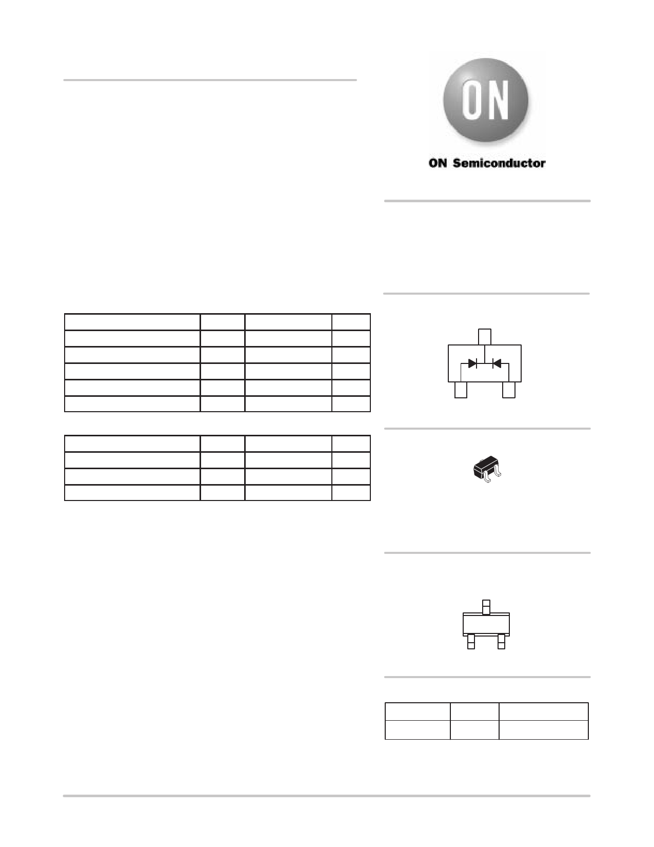
SOT–416/SC–90 PACKAGE
COMMON CATHODE
DUAL SWITCHING DIODE
SURFACE MOUNT
CATHODE
3
12
ANODE
3
2
1
SOT–416
CASE 463
STYLE 3
DEVICE MARKING
N9
ORDERING INFORMATION
Device
Package
Shipping
DAN222
SOT–416 3000/Tape & Reel
© Semiconductor Components Industries, LLC, 2000
March, 2000 – Rev. 2
1
Publication Order Number:
DAN222/D
1 page 
DAN222
INFORMATION FOR USING THE SOT-416 SURFACE MOUNT PACKAGE
MINIMUM RECOMMENDED FOOTPRINT FOR SURFACE MOUNTED APPLICATIONS
Surface mount board layout is a critical portion of the
total design. The footprint for the semiconductor packages
must be the correct size to insure proper solder connection
interface between the board and the package. With the
correct pad geometry, the packages will self align when
subjected to a solder reflow process.
TYPICAL
SOLDERING PATTERN
Unit: mm
0.5
ÉÉÉÉÉÉÉÉÉ
min. (3x)
1.4
ÉÉÉÉÉÉÉÉÉ
ÉÉÉÉÉÉÉÉÉ
SOT–416/SC–90 POWER DISSIPATION
The power dissipation of the SOT–416/SC–90 is a
function of the pad size. This can vary from the minimum
pad size for soldering to the pad size given for maximum
power dissipation. Power dissipation for a surface mount
device is determined by TJ(max), the maximum rated
junction temperature of the die, RθJA, the thermal
resistance from the device junction to ambient; and the
operating temperature, TA. Using the values provided on
the data sheet, PD can be calculated as follows.
PD =
TJ(max) – TA
RθJA
The values for the equation are found in the maximum
ratings table on the data sheet. Substituting these values
into the equation for an ambient temperature TA of 25°C,
one can calculate the power dissipation of the device which
in this case is 125 milliwatts.
PD =
150°C – 25°C
833°C/W
= 150 milliwatts
The 833°C/W assumes the use of the recommended
footprint on a glass epoxy printed circuit board to achieve a
power dissipation of 150 milliwatts. Another alternative
would be to use a ceramic substrate or an aluminum core
board such as Thermal Clad™. Using a board material such
as Thermal Clad, a higher power dissipation can be
achieved using the same footprint.
SOLDERING PRECAUTIONS
The melting temperature of solder is higher than the rated
temperature of the device. When the entire device is heated
to a high temperature, failure to complete soldering within
a short time could result in device failure. Therefore, the
following items should always be observed in order to
minimize the thermal stress to which the devices are
subjected.
• Always preheat the device.
• The delta temperature between the preheat and
soldering should be 100°C or less.*
• When preheating and soldering, the temperature of the
leads and the case must not exceed the maximum
temperature ratings as shown on the data sheet. When
using infrared heating with the reflow soldering
method, the difference should be a maximum of 10°C.
• The soldering temperature and time should not exceed
260°C for more than 10 seconds.
• When shifting from preheating to soldering, the
maximum temperature gradient should be 5°C or less.
• After soldering has been completed, the device should
be allowed to cool naturally for at least three minutes.
Gradual cooling should be used as the use of forced
cooling will increase the temperature gradient and
result in latent failure due to mechanical stress.
• Mechanical stress or shock should not be applied
during cooling
* Soldering a device without preheating can cause
excessive thermal shock and stress which can result in
damage to the device.
http://onsemi.com
5
5 Page | ||
| Páginas | Total 8 Páginas | |
| PDF Descargar | [ Datasheet DAN222.PDF ] | |
Hoja de datos destacado
| Número de pieza | Descripción | Fabricantes |
| DAN222 | SOT-416/SC-90 PACKAGE COMMON CATHODE DUAL SWITCHING DIODE SURFACE MOUNT | Motorola Inc |
| DAN222 | COMMON CATHODE SILICON DUAL SWITCHING DIODE | ON Semiconductor |
| DAN222 | Ultra high speed switching | Diodes Incorporated |
| DAN222 | Band Switching Diode | ROHM Semiconductor |
| Número de pieza | Descripción | Fabricantes |
| SLA6805M | High Voltage 3 phase Motor Driver IC. |
Sanken |
| SDC1742 | 12- and 14-Bit Hybrid Synchro / Resolver-to-Digital Converters. |
Analog Devices |
|
DataSheet.es es una pagina web que funciona como un repositorio de manuales o hoja de datos de muchos de los productos más populares, |
| DataSheet.es | 2020 | Privacy Policy | Contacto | Buscar |