|
|
|
PDF AD7886 Data sheet ( Hoja de datos )
| Número de pieza | AD7886 | |
| Descripción | LC2MOS 12-Bit/ 750 kHz/1 MHz/ Sampling ADC | |
| Fabricantes | Analog Devices | |
| Logotipo | ||
Hay una vista previa y un enlace de descarga de AD7886 (archivo pdf) en la parte inferior de esta página. Total 16 Páginas | ||
|
No Preview Available !
a
LC2MOS
12-Bit, 750 kHz/1 MHz, Sampling ADC
AD7886
FEATURES
750 kHz/1 MHz Throughput Rate
1 s/750 ns Conversion Time
12-Bit No Missed Codes Over Temperature
67 dB SNR at 100 kHz Input Frequency
Low Power—250 mW typ
Fast Bus Access Time—57 ns max
APPLICATIONS
Digital Signal Processing
Speech Recognition and Synthesis
Spectrum Analysis
DSP Servo Control
GENERAL DESCRIPTION
The AD7886 is a 12-bit ADC with a sample-and-hold amplifier
offering high speed performance combined with low power dissi-
pation. The AD7886 is a triple pass flash ADC that uses 15
comparators in a 4-bit flash technique to achieve 12-bit accuracy
in 1 µs/750 ns conversion time. An on-chip clock oscillator pro-
vides the appropriate timing for each of the three conversion
stages, eliminating the need for any external clocks. Acquisition
time of the sample-and-hold amplifier gives a resulting through-
put rate of 750 kHz/1 MHz.*
The AD7886 operates from ± 5 V power supplies. Pin-strappable
inputs offer a choice of three analog input ranges: 0 V to 5 V,
0 V to 10 V or ± 5 V.
In addition to the traditional dc accuracy specifications such as
linearity, offset and full-scale errors, the AD7886 is also speci-
fied for dynamic performance parameters, including harmonic
distortion and signal-to-noise ratio.
The AD7886 has a high speed digital interface with three-state
data outputs. Conversion control is provided by a CONVST in-
put. Data access is controlled by CS and RD inputs, standard
microprocessor signals. The data access time of less than 57 ns
means that the AD7886 can interface directly to most modern
microprocessors, including DSP processors.
*Contact your local salesperson for further information on the 1 MHz
version.
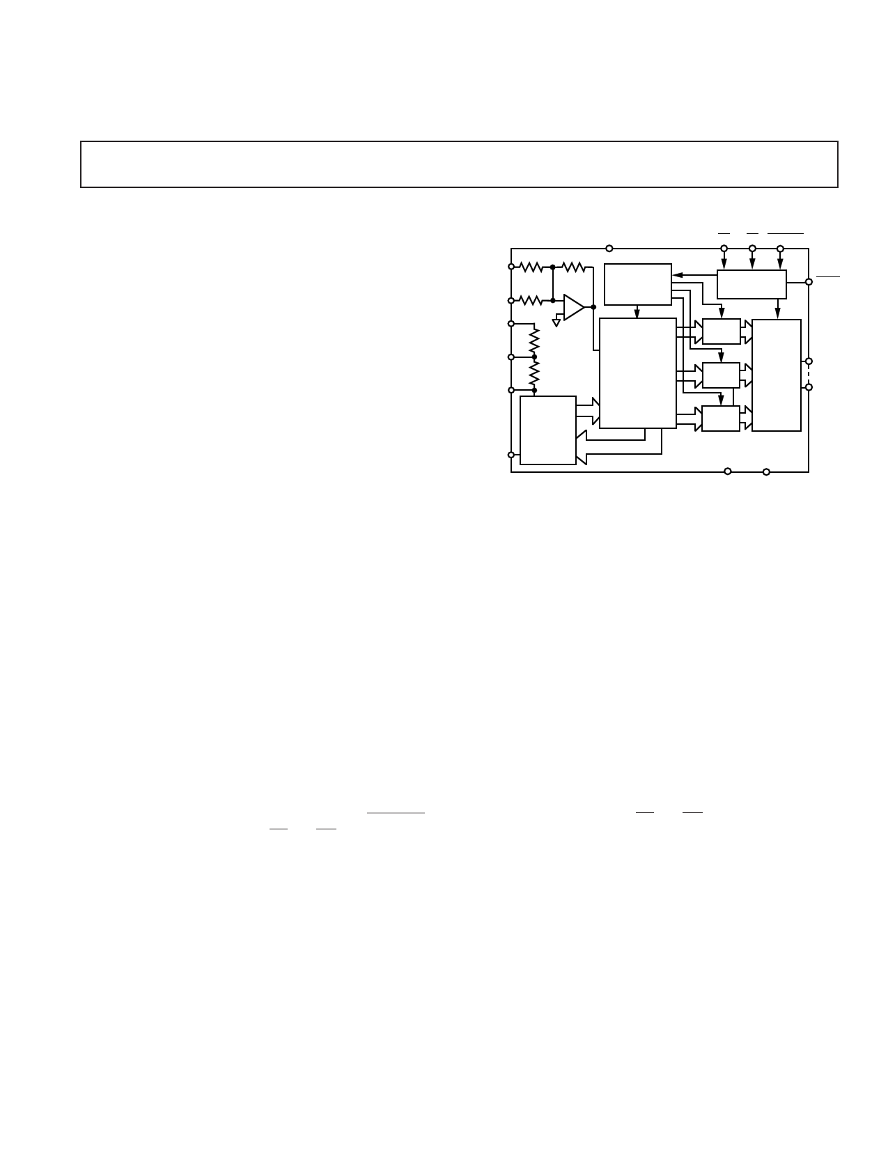
FUNCTIONAL BLOCK DIAGRAM
VIN1
VIN2
+5REF
SUM
VREF
AGND
VDD
R3 R5
10k
R4
10k
R1
9k
3.5k
–
+
T/H
R2
6.3k
CLOCK
OSCILLATOR
AND TIMER
15
COMPARATORS
AND
4-BIT FLASH
LOGIC
4096
RESISTOR
DAC
SEGMENT SELECT
CS RD CONVST
CONTROL
TIMER
BUSY
4-BIT
LATCH
4-BIT
LATCH
4-BIT
LATCH
THREE
STATE
OUTPUTS
AD7886
DB11
DB0
VSS DGND
The AD7886 is fabricated in Analog Devices’ Linear Com-
patible CMOS process, a mixed technology process that
combines precision bipolar circuits with low power CMOS
logic.
The AD7886 is available in both a 28-pin DIP and a 28-pin
leaded chip carrier.
PRODUCT HIGHLIGHTS
1. Fast 1.33 µs/1 µs Throughput Time.
Fast throughput time makes the AD7886 suitable for a
wide range of data acquisition applications.
2. Dynamic Specifications for DSP Users.
The AD7886 is specified for ac parameters, including
signal-to-noise ratio, harmonic distortion and inter-
modulation distortion. Key digital timing parameters are
also tested and guaranteed over the full operating tem-
perature range.
3. Fast Microprocessor Interface.
Standard control signals, CS and RD, and fast bus ac-
cess times make the AD7886 easy to interface to micro-
processors.
4. Low Power.
LC2MOS fabrication process gives low power dissipa-
tion of 250 mW.
REV. B
Information furnished by Analog Devices is believed to be accurate and
reliable. However, no responsibility is assumed by Analog Devices for its
use, nor for any infringements of patents or other rights of third parties
which may result from its use. No license is granted by implication or
otherwise under any patent or patent rights of Analog Devices.
One Technology Way, P.O. Box 9106, Norwood, MA 02062-9106, U.S.A.
Tel: 617/329-4700 World Wide Web Site: http://www.analog.com
Fax: 617/326-8703
© Analog Devices, Inc., 1997
1 page 
AD7886
PIN CONFIGURATIONS
DIP PLCC
DB7 1
DB6 2
DB5 3
DB4 4
DGND 5
DB3 6
DB2 7
DB1 8
DB0 9
VDD 10
BUSY 11
CS 12
RD 13
CONVST 14
AD7886
TOP VIEW
(Not to Scale)
28 DB8
27 DB9
26 DB10
25 DB11
24 VSS
23 AGND
22 VREF
21 SUM
20 +5REF
19 VDD
18 VIN2
17 VIN1
16 AGND
15 VSS
4 3 2 1 28 27 26
DGND 5
DB3 6
DB2 7
DB1 8
DB0 9
VDD 10
BUSY 11
AD7886
TOP VIEW
(Not to Scale)
25 DB11
24 VSS
23 AGND
22 VREF
21 SUM
20 +5REF
19 VDD
12 13 14 15 16 17 18
TERMINOLOGY
Unipolar Offset Error
The ideal first code transition should occur when the analog
input is 1 LSB above AGND. The deviation of the actual transi-
tion from that point is termed the offset error.
Bipolar Zero Error
The ideal midscale transition (i.e., 0111 1111 1111 to 1000
0000 0000) for the +5 V range should occur when the analog
input is at zero volts. Bipolar zero error is the deviation of the
actual transition from that point.
Gain Error
In the unipolar mode, gain error is measured with respect to the
first and last code transition points. The ideal difference be-
tween these points is FS–2 LSBs. For bipolar applications, the
gain error is measured from the midscale transition to both the
first and last code transitions. The ideal difference in this case is
FS/2–1 LSB. The gain error is defined as the deviation between
the ideal difference, given above, and the measured difference.
For the bipolar case, there are two gain errors; the figure in the
specification page represents the worst case. Ideal FS depends
on the +5REF input; for the 0 V to 5 V input, ideal FS = +5REF
and for the 0 V to 10 V and +5 V ranges, ideal FS = 2 × + 5REF.
result. The 12 bits of data are then stored internally in a three-
state output latch.
REFERENCE INPUT
The AD7886 operates from a 3.5 V reference, which must be
provided at the VREF input. Two on-chip resistors for use with
an external amplifier can be used for deriving 3.5 V from stan-
dard 5 V references. Figure 2 shows an example with the AD586
which a is a high performance voltage reference exhibiting
excellent stability performance, 5 ppm/°C max. The external
amplifier serves a second function of force/sensing the VREF
input. Force/sensing minimizes error contributions from
+V
+VIN
VOUT +5V
AD586
GND
+5REF
SUM
R1
9k
AD7886*
CONVERTER DETAILS
The AD7886 is a triple-pass flash ADC that uses 15 compara-
tors in a 4-bit flash technique to perform the 12-bit conversion
procedure. Each of the 4096 quantization levels is realized inter-
nally with a precision resistor DAC.
The fifteen comparators first compare the analog input voltage
to the VREF/16 voltages of the resistor array. This determines the
four most significant bits and selects 1 out of 16 voltage seg-
ments. The comparators are then switched to 15 subvoltages on
that segment to determine the next four bits and select 1 out of
256 voltage segments. A further switching of the comparators to
another 15 subvoltages produces the complete 12-bit conversion
AD707
– –3.5V
+
C1
10µF
C2
0.1µF
VREF
R2
6.3k
TO DAC
AGND
*ADDITIONAL PINS OMITTED FOR CLARITY
Figure 2. Typical Reference Circuitry
REV. B
–5–
5 Page 
AD7886
CLK
OUT
DMA13
DMA0
ADDRESS BUS
TIMER
DMS
DMACK
ADSP-2100
ADDR
ENCODE
EN
CONVST
CS
Q CLR
74HC74 D
CLK
AD7886*
+ 5V
IRQn
DMRD
BUSY
RD
DB11
DB0
DMD15
DMD0
DATA BUS
*ADDITIONAL PINS OMITTED FOR CLARITY
Figure 17. AD7886–ADSP-2100 Interface
A15
A0
TMS320C25
IS
ADDRESS BUS
ADDR
ENCODE
EN
TIMER
CONVST
CS
READY
G2
AD7886*
MSC
STRB
R/W
RD
INT BUSY
DB11
DB0
D15
DATA BUS
D0
*ADDITIONAL PINS OMITTED FOR CLARITY
Figure 18. AD7886–TMS320C25 Interface
A15
ADDRESS BUS
A0
X/Y EN1 ADDR
ENCODE
DS EN2
TIMER
CONVST
CS
RD
IRQ BUSY
RD
DSP56000
OE CLK
Q11 D11
Q0 D0
2X
74HC374
AD7886*
DB11
DB0
D23
DATA BUS
D0
*ADDITIONAL PINS OMITTED FOR CLARITY
Figure 19. AD7886–DSP56000 Interface
REV. B
AD7886–MC68000
Applications requiring conversions to be initiated by the micro-
processor rather than an external timer may decode a CONVST
signal from the address bus. An example is given in Figure 20
with the MC68000 processor. A write instruction starts conver-
sion while a read instruction reads the data when conversion is
complete. A delay at least as long as the ADC conversion time
must be allowed between initiating a conversion and reading the
ADC data into the processor. In Figure 20, BUSY is used to
drive the processor into a WAIT state if the processor attempts
to read data before conversion is complete.
Conversion is initiated with a write instruction to the ADC:
Move.W D0,ADC
(ADC = ADC address)
Data is transferred to the processor with a read instruction;
BUSY will force the processor to WAIT for the end of conver-
sion if a conversion is in progress.
Move.W ADC,DO
(ADC = ADC address)
A15
ADDRESS BUS
A0
ADDR
ENCODE
AS EN
CS
CONVST
R/W
DTACK
RD
BUSY
AD7886*
MC68000
DB11
DB0
D11
DATA BUS
D0
*ADDITIONAL PINS OMITTED FOR CLARITY
Figure 20. AD7886–MC68000 Interface
AD7886–Z-80/8085A
For 8-bit processors, an external latch is required to store four
bits of the conversion result (4 LSBs in Figure 21). The data is
then read in two bytes: one read from the ADC and a second
from the latch.
Figure 21 shows a typical interface suitable for the Z-80 or the
8085A. Not shown in the Figure is the 8-bit latch needed to
demultiplex the 8085A common address/data bus. The follow-
ing LOAD instruction reads the conversion result into the HL
register pair:
For the 8085A–LHLD
For the Z-80–LDHL
(ADC) (ADC = ADC address)
(ADC) (ADC = ADC address)
This is a two byte read instruction. The first byte to be read has
to be the high byte (DB11 to DB4). At the end of the first read
operation, the rising edge of CS and RD clocks the 4 LSBs into
74HC374 latches. The second byte (4 LSBs) is then read from
these latches.
–11–
11 Page | ||
| Páginas | Total 16 Páginas | |
| PDF Descargar | [ Datasheet AD7886.PDF ] | |
Hoja de datos destacado
| Número de pieza | Descripción | Fabricantes |
| AD7880 | LC2MOS Single +5 V Supply/ Low Power/ 12-Bit Sampling ADC | Analog Devices |
| AD7883 | LC2MOS 12-Bit/ 3.3 V Sampling ADC | Analog Devices |
| AD7884 | LC2MOS 16-Bit/ High Speed Sampling ADCs | Analog Devices |
| AD7885 | LC2MOS 16-Bit/ High Speed Sampling ADCs | Analog Devices |
| Número de pieza | Descripción | Fabricantes |
| SLA6805M | High Voltage 3 phase Motor Driver IC. |
Sanken |
| SDC1742 | 12- and 14-Bit Hybrid Synchro / Resolver-to-Digital Converters. |
Analog Devices |
|
DataSheet.es es una pagina web que funciona como un repositorio de manuales o hoja de datos de muchos de los productos más populares, |
| DataSheet.es | 2020 | Privacy Policy | Contacto | Buscar |