|
|
|
PDF AD7873 Data sheet ( Hoja de datos )
| Número de pieza | AD7873 | |
| Descripción | Touch Screen Digitizer | |
| Fabricantes | Analog Devices | |
| Logotipo | ||
Hay una vista previa y un enlace de descarga de AD7873 (archivo pdf) en la parte inferior de esta página. Total 28 Páginas | ||
|
No Preview Available !
FEATURES
4-wire touch screen interface
On-chip temperature sensor: −40°C to +85°C
On-chip 2.5 V reference
Direct battery measurement (0 V to 6 V)
Touch-pressure measurement
Specified throughput rate of 125 kSPS
Single supply, VCC of 2.2 V to 5.25 V
Ratiometric conversion
High speed serial interface
Programmable 8-bit or 12-bit resolution
One auxiliary analog input
Shutdown mode: 1 µA max
16-lead QSOP, TSSOP, and LFCSP packages
APPLICATIONS
Personal digital assistants
Smart hand-held devices
Touch screen monitors
Point-of-sale terminals
Pagers
GENERAL DESCRIPTION
The AD7873 is a 12-bit successive approximation ADC with a
synchronous serial interface and low on resistance switches for
driving touch screens. The AD7873 operates from a single 2.2 V
to 5.25 V power supply and features throughput rates greater
than 125 kSPS.
The AD7873 features direct battery measurement, temperature
measurement, and touch-pressure measurement. The AD7873
also has an on-board reference of 2.5 V that can be used for the
auxiliary input, battery monitor, and temperature measurement
modes. When not in use, the internal reference can be shut
down to conserve power. An external reference can also be
applied and can be varied from 1 V to VCC, while the analog
input range is from 0 V to VREF. The device includes a shutdown
mode that reduces the current consumption to less than 1 µA.
The AD7873 features on-board switches. This, coupled with low
power and high speed operation, makes the device ideal for
battery-powered systems such as personal digital assistants with
resistive touch screens and other portable equipment. The part
is available in a 16-lead 0.15" quarter size outline package
(QSOP), a 16-lead thin shrink small outline package (TSSOP),
and a 16-lead lead frame chip scale package (LFCSP).
Rev. D
Information furnished by Analog Devices is believed to be accurate and reliable.
However, no responsibility is assumed by Analog Devices for its use, nor for any
infringements of patents or other rights of third parties that may result from its use.
Specifications subject to change without notice. No license is granted by implication
or otherwise under any patent or patent rights of Analog Devices. Trademarks and
registered trademarks are the property of their respective owners.
Touch Screen Digitizer
AD7873
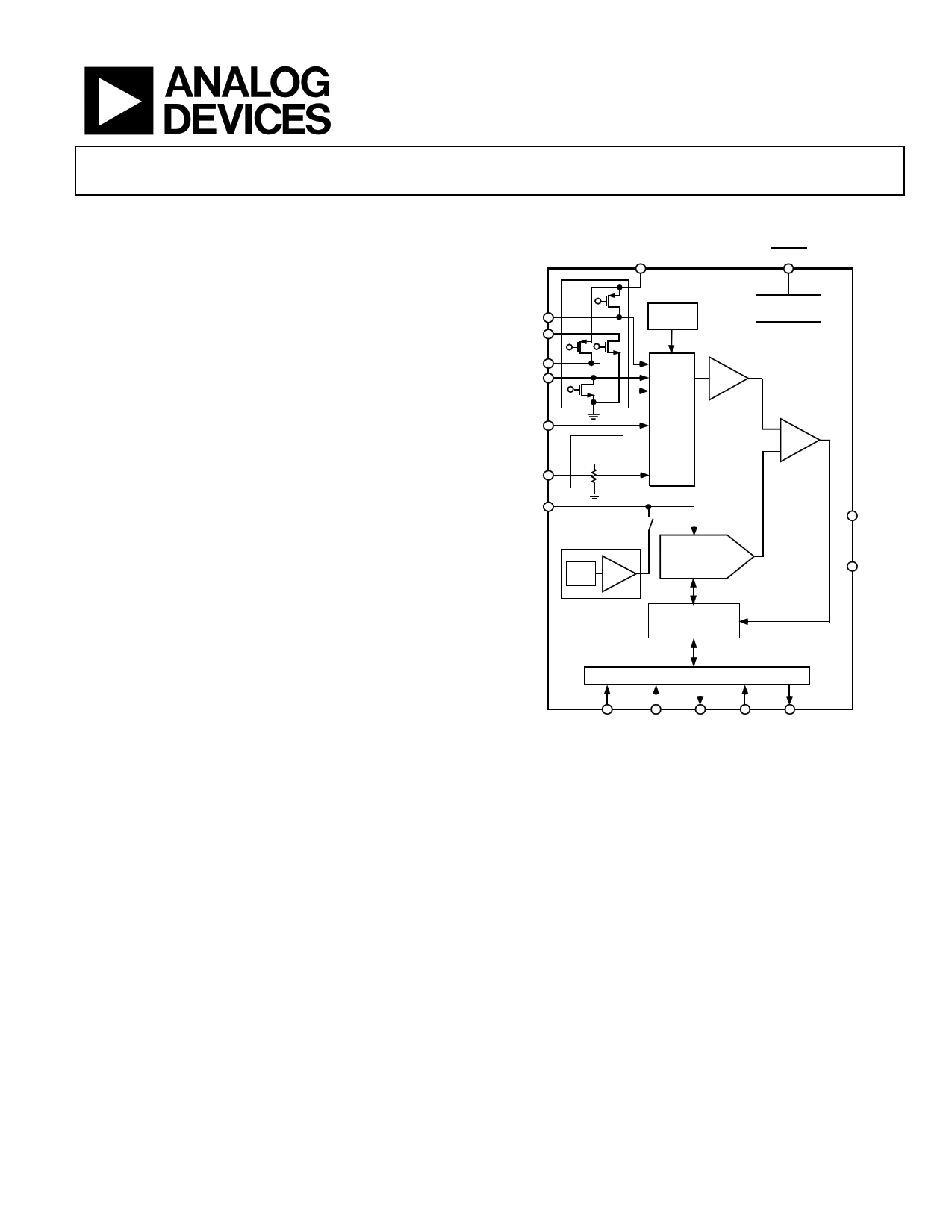
FUNCTIONAL BLOCK DIAGRAM
+VCC
PENIRQ
X+
X–
Y+
Y–
AUX
VBAT
VREF
BATTERY
MONITOR
TEMP
SENSOR
6-TO-1
I/P
MUX
T/H
PEN
INTERRUPT
AD7873
COMP
2.5V
REF
BUF
CHARGE
REDISTRIBUTION
DAC
SAR + ADC
CONTROL LOGIC
GND
+VCC
SPORT
DIN CS DOUT DCLK BUSY
Figure 1.
PRODUCT HIGHLIGHTS
1. Ratiometric conversion mode available, eliminating errors
due to on-board switch resistances.
2. On-board temperature sensor: −40°C to +85°C.
3. Battery monitor input.
4. Touch-pressure measurement capability.
5. Low power consumption of 1.37 mW max with the
reference off, or 2.41 mW typ with the reference on, at
125 kSPS and VCC at 3.6 V.
6. Package options include 4 mm × 4 mm LFCSP.
7. Analog input range from 0 V to VREF.
8. Versatile serial I/O ports.
One Technology Way, P.O. Box 9106, Norwood, MA 02062-9106, U.S.A.
Tel: 781.329.4700
www.analog.com
Fax: 781.326.8703 © 2004 Analog Devices, Inc. All rights reserved.
1 page 
AD7873
TIMING SPECIFICATIONS
TA = TMIN to TMAX, unless otherwise noted; VCC = 2.7 V to 5.25 V, VREF = 2.5 V.
Table 2. Timing Specifications1
Parameter
Limit at TMIN, TMAX
fDCLK2
10
2
tACQ 1.5
t1 10
t2 60
t33 60
t4 200
t5 200
t6 60
t7 10
t8 10
t93 200
t10 0
t11 100
t124 100
Unit
kHz min
MHz max
µs min
ns min
ns max
ns max
ns min
ns min
ns max
ns min
ns min
ns max
ns min
ns max
ns max
Description
Acquisition time
CS falling edge to first DCLK rising edge
CS falling edge to busy three-state disabled
CS falling edge to DOUT three-state disabled
DCLK high pulse width
DCLK low pulse width
DCLK falling edge to BUSY rising edge
Data setup time prior to DCLK rising edge
Data valid to DCLK hold time
Data access time after DCLK falling edge
CS rising edge to DCLK ignored
CS rising edge to BUSY high impedance
CS rising edge to DOUT high impedance
1 Sample tested at 25°C to ensure compliance. All input signals are specified with tr = tf = 5 ns (10% to 90% of VCC) and timed from a voltage level of 1.6 V.
2 Mark/Space ratio for the DCLK input is 40/60 to 60/40.
3 Measured with the load circuit of Figure 2 and defined as the time required for the output to cross 0.4 V or 2.0 V.
4 t12 is derived from the measured time taken by the data outputs to change 0.5 V when loaded with the circuit of Figure 2. The measured number is then extrapolated
back to remove the effects of charging or discharging the 50 pF capacitor. This means that the time, t12, quoted in the timing characteristics is the true bus relinquish
time of the part and is independent of the bus loading.
200µA
IOL
TO
OUTPUT
PIN
CL
50pF
1.6V
200µA
IOH
Figure 2. Load Circuit for Digital Output Timing Specifications
Rev. D | Page 5 of 28
5 Page 
2.504
2.502
2.500
2.498
2.496
2.494
2.492
2.490
2.488
2.486
2.484
2.5
2.7 2.9 3.1 3.3 3.5
+VCC (V)
Figure 17. Internal VREF vs. +VCC
3.7
850
800
95.95mV
750
TEMP1
700
650
600 TEMP0
550
142.15mV
500
450
–40 –30 –20 –10 0 10 20 30 40 50 60 70 80
TEMPERATURE (°C)
Figure 18. Temp Diode Voltage vs. Temperature (2.7 V Supply)
730
729
728
727
726
725
724
723
722
721
720
2.7
3.0 3.3
VSUPPLY (V)
3.6
Figure 19. Temp 1 Diode Voltage vs. VSUPPLY (25°C)
AD7873
5
4
3
2
NO CAP (7µS)
SETTLING TIME
1
1µF CAP (1800µS)
SETTLING TIME
0
0 200 400 600 800 1000 1200 1400 1600 1800
TURN-ON TIME (µS)
Figure 20. Internal VREF vs. Turn-on Time
610
609
608
607
606
605
604
603
602
601
600
2.7 2.8 2.9 3.0 3.1 3.2 3.3 3.4 3.5 3.6
VSUPPLY (V)
Figure 21. Temp0 Diode Voltage vs. VSUPPLY (25°C)
0
fSAMPLE = 125kHz
20 fIN = 15kHz
SNR = 68.34dB
40
60
80
100
120
0
7.5 15.0 22.5 30.0 37.5 45.0 52.5 60.0
FREQUENCY (kHz)
Figure 22. Auxiliary Channel Dynamic Performance
( fSAMPLE =125 kHz, fINPUT = 15 kHz)
Rev. D | Page 11 of 28
11 Page | ||
| Páginas | Total 28 Páginas | |
| PDF Descargar | [ Datasheet AD7873.PDF ] | |
Hoja de datos destacado
| Número de pieza | Descripción | Fabricantes |
| AD7870 | LC2MOS Complete/ 12-Bit/ 100 kHz/ Sampling ADCs | Analog Devices |
| AD7870A | LC2MOS Complete/ 12-Bit/ 100 kHz / Sampling ADC | Analog Devices |
| AD7871 | LC2MOS Complete 14-Bit/ Sampling ADCs | Analog Devices |
| AD7872 | LC2MOS Complete 14-Bit/ Sampling ADCs | Analog Devices |
| Número de pieza | Descripción | Fabricantes |
| SLA6805M | High Voltage 3 phase Motor Driver IC. |
Sanken |
| SDC1742 | 12- and 14-Bit Hybrid Synchro / Resolver-to-Digital Converters. |
Analog Devices |
|
DataSheet.es es una pagina web que funciona como un repositorio de manuales o hoja de datos de muchos de los productos más populares, |
| DataSheet.es | 2020 | Privacy Policy | Contacto | Buscar |