|
|
|
PDF AD7827 Data sheet ( Hoja de datos )
| Número de pieza | AD7827 | |
| Descripción | 3 V/5 V/ 1 MSPS/ 8-Bit/ Serial Interface Sampling ADC | |
| Fabricantes | Analog Devices | |
| Logotipo | ||
Hay una vista previa y un enlace de descarga de AD7827 (archivo pdf) en la parte inferior de esta página. Total 12 Páginas | ||
|
No Preview Available !
a
3 V/5 V, 1 MSPS, 8-Bit, Serial Interface
Sampling ADC
AD7827
FEATURES
8-Bit Half-Flash ADC with 420 ns Conversion Time
200 ns Acquisition Time
8-Lead Package
On-Chip Track-and-Hold
On-Chip 2.5 V Reference with 2% Tolerance
Operating Supply Range: 3 V ؎ 10% and 5 V ؎ 10%
Specifications @ 3 V and 5 V
DSP/Microcontroller Compatible Serial Interface
Automatic Power-Down at End of Conversion
Input Ranges
0 V to 2 V, VDD = 3 V
0 V to 2.5 V, VDD = 5 V
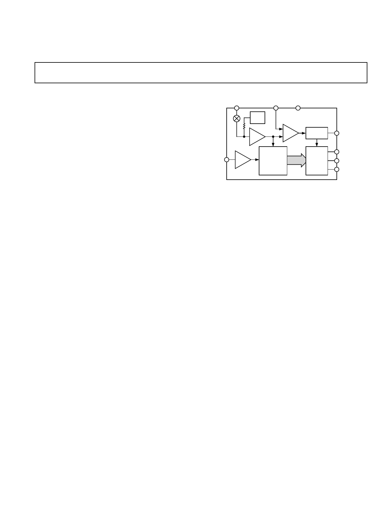
FUNCTIONAL BLOCK DIAGRAM
VREFIN/VREFOUT
VDD
GND
2.5V
REF
BUF
VDD
DETECT
COMP
AD7827
CONTROL
LOGIC
CONVST
8-BIT
VIN T/H HALF-FLASH
ADC
SERIAL
PORT
SCLK
DOUT
RFS
GENERAL DESCRIPTION
The AD7827 is a high speed, single channel, low power, analog-
to-digital converter with a maximum throughput of 1 MSPS that
operates from a single 3 V or 5 V supply. The AD7827 contains
a track/hold amplifier, an on-chip 2.5 V reference (2% toler-
ance), a 420 ns 8-bit half-flash ADC and a serial interface. The
serial interface is compatible with the serial interfaces of most
DSPs (Digital Signal Processors). The throughput rate of the
AD7827 is dependent on the clock speed of the DSP serial
interface.
The AD7827 combines the Convert Start and Power Down
signals at one pin, i.e., the CONVST pin. This allows a unique
automatic power-down at the end of a conversion to be imple-
mented. The logic level on the CONVST pin is sampled at the
end of a conversion and, depending on its state, the AD7827
powers down.
The AD7827 has one single-ended analog input with an input
span determined by the supply voltage. With a VDD of 3 V, the
input range of the AD7827 is 0 V to 2 V and with VDD equal to
5 V, the input range is 0 V to 2.5 V.
The parts are available in a small, 8-lead, 0.3" wide, plastic
dual-in-line package (DIP) and an 8-lead, small outline IC
(SOIC).
PRODUCT HIGHLIGHTS
1. Fast Conversion Time
The AD7827 has a conversion time of 420 ns. Faster conver-
sion times maximize the DSP processing time in a real time
system.
2. Built-In Track-and-Hold
The analog input signal is held and a new conversion is initi-
ated on the falling edge of the CONVST signal. The CONVST
signal allows the sampling instant to be exactly controlled.
This feature is a requirement in many DSP applications.
3. Automatic Power-Down
The CONVST signal is sampled approximately 100 ns after
the end of conversion and depending on its state the AD7827
is powered down.
4. An easy to use, fast serial interface allows direct interfacing to
most popular DSPs with no external circuitry.
REV. 0
Information furnished by Analog Devices is believed to be accurate and
reliable. However, no responsibility is assumed by Analog Devices for its
use, nor for any infringements of patents or other rights of third parties
which may result from its use. No license is granted by implication or
otherwise under any patent or patent rights of Analog Devices.
One Technology Way, P.O. Box 9106, Norwood, MA 02062-9106, U.S.A.
Tel: 781/329-4700 World Wide Web Site: http://www.analog.com
Fax: 781/326-8703
© Analog Devices, Inc., 1998
1 page 
AD7827
TERMINOLOGY
Signal-to-(Noise + Distortion) Ratio
This is the measured ratio of signal-to-(noise + distortion) at
the output of the A/D converter. The signal is the rms amplitude
of the fundamental. Noise is the rms sum of all nonfundamental
signals up to half the sampling frequency (fS/2), excluding dc.
The ratio is dependent upon the number of quantization levels in
the digitization process; the more levels, the smaller the quantiza-
tion noise. The theoretical signal-to-(noise + distortion) ratio for
an ideal N-bit converter with a sine wave input is given by:
Signal-to-(Noise + Distortion) = (6.02N + 1.76) dB
Thus for an 8-bit converter, this is 50 dB.
Total Harmonic Distortion
Total harmonic distortion (THD) is the ratio of the rms sum of
harmonics to the fundamental. For the AD7827 it is defined as:
THD (dB) = 20 log
V
2
2
+
V
2
3
+
V
2
4
+V
2
5
+V
2
6
V1
where V1 is the rms amplitude of the fundamental and V2, V3, V4,
V5 and V6 are the rms amplitudes of the second through the sixth
harmonics.
Peak Harmonic or Spurious Noise
Peak harmonic or spurious noise is defined as the ratio of the
rms value of the next largest component in the ADC output
spectrum (up to fS/2 and excluding dc) to the rms value of the
fundamental. Normally, the value of this specification is deter-
mined by the largest harmonic in the spectrum, but for parts
where the harmonics are buried in the noise floor, it will be a
noise peak.
Intermodulation Distortion
With inputs consisting of sine waves at two frequencies, fa and
fb, any active device with nonlinearities will create distortion
products at sum and difference frequencies of mfa ± nfb where
m, n = 0, 1, 2, 3, etc. Intermodulation terms are those for
which neither m nor n are equal to zero. For example, the sec-
ond order terms include (fa + fb) and (fa – fb), while the third
order terms include (2fa + fb), (2fa – fb), (fa + 2fb) and (fa – 2fb).
The AD7827 is tested using the CCIF standard where two
input frequencies near the top end of the input bandwidth are
used. In this case, the second and third order terms are of dif-
ferent significance. The second order terms are usually dis-
tanced in frequency from the original sine waves while the third
order terms are usually at a frequency close to the input fre-
quencies. As a result, the second and third order terms are
specified separately. The calculation of the intermodulation
distortion is as per the THD specification where it is the ratio
of the rms sum of the individual distortion products to the rms
amplitude of the fundamental expressed in dBs.
Relative Accuracy
Relative accuracy or endpoint nonlinearity is the maximum
deviation from a straight line passing through the endpoints of
the ADC transfer function.
Differential Nonlinearity
This is the difference between the measured and the ideal
1 LSB change between any two adjacent codes in the ADC.
Offset Error
This is the deviation of the 128th code transition (01111111) to
(10000000) from the ideal, i.e., VREF/2 (VDD = 5 V), 0.8 VREF/2
(VDD = 3 V).
Zero Scale Error
This is the deviation of the first code transition (00000000) to
(00000001) from the ideal, i.e., VREF/2 –1.25 V + 1 LSB (VDD =
5 V ± 10%), or 0.8 VREF/2 –1.0 V + 1 LSB (VDD = 3 V ± 10%).
Full-Scale Error
This is the deviation of the last code transition (11111110) to
(11111111) from the ideal, i.e., VMID + 1.25 V – 1 LSB (VDD =
5 V ± 10%), or VMID + 1.0 V – 1 LSB (VDD = 3 V ± 10%).
Gain Error
This is the deviation of the last code transition (1111 . . . 110) to
(1111 . . . 111) from the ideal, i.e., VREF – 1 LSB, after the offset
error has been adjusted out.
Track/Hold Acquisition Time
Track/hold acquisition time is the time required for the output
of the track/hold amplifier to reach its final value, within
± 1/2 LSB, after the point at which the track/hold returns to
track mode. This happens approximately 120 ns after the falling
edge of CONVST.
It also applies when there is a step input change on the input
voltage applied to the VIN input of the AD7827. It means that
the user must wait for the duration of the track/hold acquisition
time after the end of conversion or after a step input change to
VIN before starting another conversion, to ensure that the part
operates to specification.
REV. 0
–5–
5 Page 
AD7827
MICROPROCESSOR INTERFACING
The Serial Interface on the AD7827 allows the part to be con-
nected directly to a range of many different microprocessors and
microcontrollers. This section explains how to interface the
AD7827 with some of the more common DSP serial interface
protocols.
AD7827 to TMS320C5x
The serial interface on the TMS320C5x uses a continuous serial
clock and frame synchronization signals to synchronize the data
transfer operations with peripheral devices such as the AD7827.
A receive frame synchronization output has been supplied on
the AD7827 to allow easy interfacing with no extra gluing logic.
The serial port of the TMS320C5x is set up to operate in Burst
Mode with internal CLKX (TX serial clock) and FSR (RX
frame sync). The Serial Port Control register (SPC) must have
the following setup: F0 = 1, FSM = 1, MCM = 1. The connec-
tion diagram is shown in Figure 16.
AD7827*
SCLK
DOUT
RFS
TMS320C5x*
CLKX
CLKR
DR
FSR
AD7827 to DSP56xxx
The connection diagram in Figure 18 shows how the AD7827
can be connected to the SSI (Synchronous Serial Interface) of
the DSP56xxx family of DSPs from Motorola. The SSI is oper-
ated in Synchronous Mode (SYN bit in CRB = 1) with inter-
nally generated 1-bit clock period frame sync for both TX and
RX (FSL1 and FSL0 bits in CRB = 1 and 0 respectively).
AD7827*
SCLK
DOUT
RFS
DSP56xxx*
SCLK
SRD
SC2
*ADDITIONAL PINS OMITTED FOR CLARITY
Figure 18. Interfacing to the DSP56xxx
Microcontrollers
The AD7827 may also be interfaced to many microcontrollers,
as a continuous serial clock is not essential. However, enough
time must be left for the conversion to be complete before
applying a burst of serial clocks to read out the data.
*ADDITIONAL PINS OMITTED FOR CLARITY
Figure 16. Interfacing to the TMS320C5x
AD7827 to ADSP-21xx
The ADSP-21xx family of DSPs are easily interfaced to the
AD7827 without the need for any extra gluing logic. The
SPORT is operated in alternate framing mode. The SPORT
control register should be set up as follows:
TFSW = RFSW = 1, Alternate Framing
INVRFS = INVTFS = 1, Active Low Frame Signal
DTYPE = 00, Right Justify Data
SLEN = 0111, 8-Bit Data Words
ISCLK = 1, Internal Serial Clock
TFSR = RFSR = 1, Frame Every Word
IRFS = 0, External Framing Signal
ITFS = 1, Internal Framing Signal
The 8-bit data words will be right justified in the 16-bit serial
data registers when using this configuration. Figure 17 shows
the connection diagram.
AD7827*
SCLK
DOUT
RFS
ADSP-21xx*
SCLK
DR
RFS
*ADDITIONAL PINS OMITTED FOR CLARITY
Figure 17. Interfacing to the ADSP-21xx
REV. 0
–11–
11 Page | ||
| Páginas | Total 12 Páginas | |
| PDF Descargar | [ Datasheet AD7827.PDF ] | |
Hoja de datos destacado
| Número de pieza | Descripción | Fabricantes |
| AD7820 | 8-BIT ADC | Analog Devices |
| AD7821 | LC2MOS High Speed/ mP-Compatible 8-Bit ADC with Track/Hold Function | Analog Devices |
| AD7822 | 3 V/5 V/ 2 MSPS/ 8-Bit/ 1-/ 4-/ 8-Channel Sampling ADCs | Analog Devices |
| AD7823 | 2.7 V to 5.5 V/ 4.5 us/ 8-Bit ADC in 8-Lead microSOIC/DIP | Analog Devices |
| Número de pieza | Descripción | Fabricantes |
| SLA6805M | High Voltage 3 phase Motor Driver IC. |
Sanken |
| SDC1742 | 12- and 14-Bit Hybrid Synchro / Resolver-to-Digital Converters. |
Analog Devices |
|
DataSheet.es es una pagina web que funciona como un repositorio de manuales o hoja de datos de muchos de los productos más populares, |
| DataSheet.es | 2020 | Privacy Policy | Contacto | Buscar |