|
|
|
PDF ADM1014 Data sheet ( Hoja de datos )
| Número de pieza | ADM1014 | |
| Descripción | Dual PCI Hot-PlugTM Controller | |
| Fabricantes | Analog Devices | |
| Logotipo | ||
Hay una vista previa y un enlace de descarga de ADM1014 (archivo pdf) en la parte inferior de esta página. Total 12 Páginas | ||
|
No Preview Available !
=
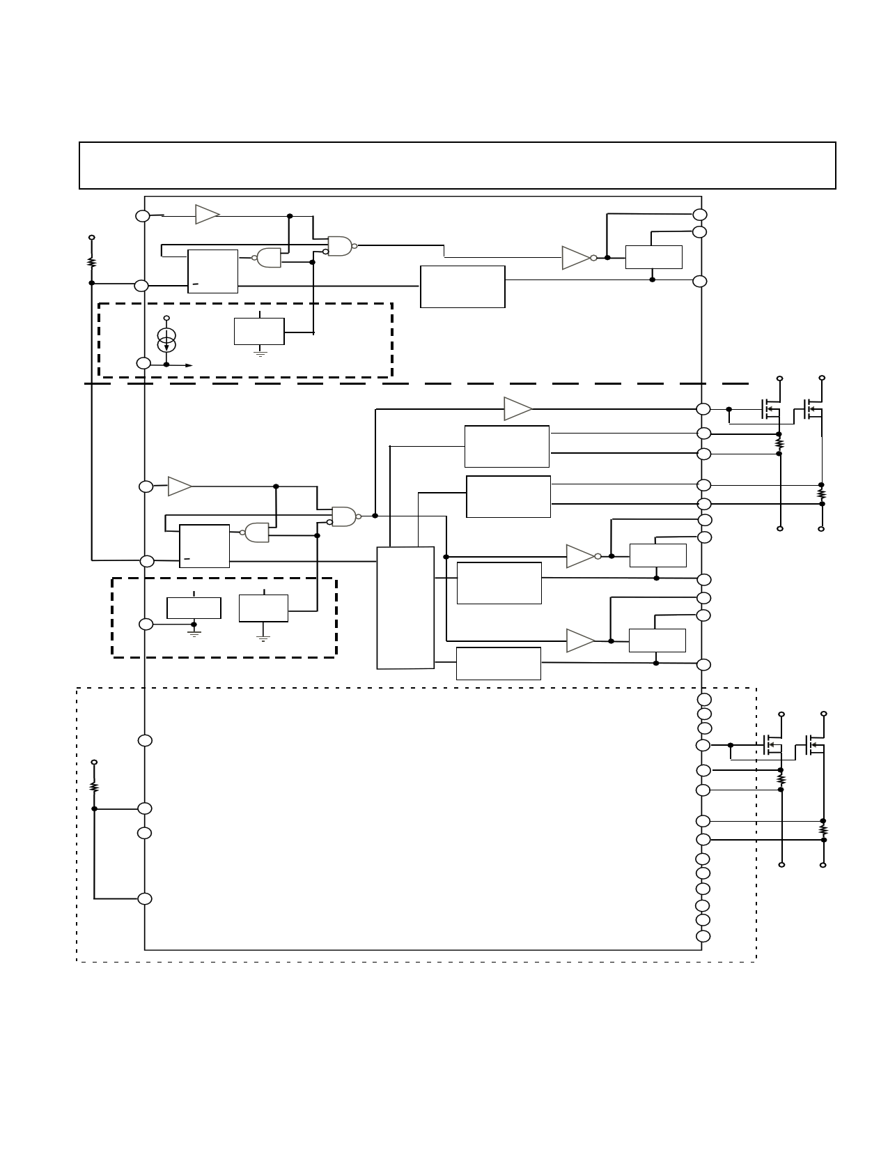
Dual PCI Hot-PlugTM Controller
Preliminary Technical Data
ADM1014
3.3V Cmos
PAUXONA 30
Input
+3.3VAux
FAUXA
Q RESET
3.3V Cmos FAULT
Output
LATCH
5 Q SET
AUXINA
AUXINA
100µA
3.3VAUX
POWER-ON
RESET
LOW WHEN
AUXINA < 2.5V
OCSET 6
VOCSET
COMMON TO BOTH CHANNELS
OVERCURRENT AND
UNDERVOLTAGE
COMPARATORS
FOR +3.3VAUX
S
G P-CHANNEL
MOSFET
D
7 AUXGA
31 AUXINA
8 AUXOA
CHANNEL A
CIRCUIT OPERATES FROM 3.3VAUX POWER SUPPLY
CIRCUIT OPERATES FROM 3.3VAUX AND +12V POWER SUPPLY
3V5VGA
33
EXTERNAL
N-CHANNEL
POWER
MOSFETS
+5V
IN
+3.3V
IN
CHANNEL A
OVERCURRENT AND
UNDERVOLTAGE
COMPARATORS
FOR +5V
34 5VSA
5VISENA
35
RSENSE5A
PWRONA 3
FLTNA
4
Q RESET
FAULT
LATCH
Q SET
GND
12VIN
A
5V
REGULATOR
12VIN
A
12V IN
POWER-ON
RESET
32 LOW WHEN
12VINA <
10V
COMMON TO BOTH CHANNELS
OVERCURRENT AND
UNDERVOLTAGE
COMPARATORS
FOR +3.3V
COMBINING
LOGIC
OVERCURRENT AND
UNDERVOLTAGE
COMPARATORS
FOR +12V
OVERCURRENT
COMPARATOR
FOR -12V
PAUXONB 27
+3.3VAux
FAUXB
15
PWRONB 17
FLTNB
16
CHANNEL B
( IDENTICAL TO CHANNEL A )
S
G P-CHANNEL
MOSFET
D
S
G N-CHANNEL
MOSFET
D
36 3VSA
3VISENA
37
9 12VGA
29 12VIN
A
RSENSE3A
+5V
OUTA
+3.3V
OUTA
10 12VOA
2 -12VGA
38 -12VINA
1 -12VOA
14 AUXGB
26 AUXINB
13 AUXOB
3V5VGB
25
EXTERNAL
N-CHANNEL
POWER
MOSFETS
+5V
IN
+3.3V
IN
5VSB
24
5VISENB
23
RSENSE5B
3VSB
22
3VISENB
21
12 12VGB
28 12VINB
11 12VOB
18 -12VGB
20 -12VINB
19 -12VOB
RSENSE3B
+5V
OUTA
+3.3V
OUTA
REV. PrN 1/02
FUNCTIONAL BLOCK DIAGRAM
Information furnished by Analog Devices is believed to be accurate and
reliable. However, no responsibility is assumed by Analog Devices for its
use, nor for any infringements of patents or other rights of third parties
which may result from its use. No license is granted by implication or
otherwise under any patent or patent rights of Analog Devices.
TM Hot Plug is a trademark of Core International, Inc.
One Technology Way, P.O. Box 9106, Norwood, MA 02062-9106, U.S.A.
Tel: 781/329-4700
www.analog.com
Fax: 781/326-8703
© Analog Devices, Inc., 2002
1 page 
ADM1014
PIN FUNCTION DESCRIPTION
Pin Mnemonic Function
1
M12VOA
Switched -12V output for channel A. Rated for 100mA.
2
M12VGA
Gate of channel A internal NMOS transistor. A capacitor connected from this pin to -12VOA (pin 1)
sets the start-up ramp for the +12V supply. During turn-on, this capacitor is charged from a 25µA
current source.
3 PWRONA Power on control for channel A. 3.3V CMOS-compatible logic input controls all four main supplies.
PWRONA high = outputs on, PWRONA low = outputs off.
4 FLTNA Active-low, 5V compatible, Open Drain fault output for channel A. A pull-up resistor connects the
pin to 3.3VAux. 4.7k⍀ is recommended for this function. An optional capacitor may be connected
from this pin to GND to provide improved immunity to power supply transients.
5 FAUXA Active-low, 3.3V compatible, Open Drain fault output for Aux channel A. The same pull-up resistor
as that on FLTNA connects the pin to 3.3VAux.
6 OCSET Overcurrent set for all 10 outputs. A resistor connected from this pin to ground sets the overcurrent
trip point of all eight supplies. All eight overcurrent trip-points can be programmed by changing the
value of this resistor. The default value of 6.04k⍀, ±1% is compatible with the maximum currents
allowed by the PCI specification.
7 AUXGA Gate of channel A +3.3VAUX internal PMOS transistor. A capacitor connected from this pin to
AUXOA (pin 8) sets the start-up ramp for the +3.3VAUX supply. During turn-on, this capacitor is
charged from a 25µA current source.
8 AUXOA Switched 3.3V auxiliary output for channel A. Rated for 0.375A.
9 12VGA
Gate of channel A internal PMOS transistor. A capacitor connected from this pin to 12VOA (pin 10)
sets the start-up ramp for the +12V supply. During turn-on, this capacitor is charged from a 25µA
current source. The undervoltage circuitry is disabled when the voltage on 12VGA rises above 1.2V.
If the capacitor on pin 7 (AUXGA) or pin 33 (3V5VGA) is more than 25% larger than the capacitor on
pin 9 (12VGA) a false undervoltage condition may be detected during startup.
10 12VOA
Switched 12V output for channel A. Rated for 0.5A.
11 12VOB
Switched 12V output for channel B. Rated for 0.5A.
12 12VGB
Gate of channel B internal PMOS transistor. A capacitor connected from this pin to 12VOB (pin 11)
sets the start-up ramp for the +12V supply. During turn-on, this capacitor is charged from a 25µA
current source. The undervoltage circuitry is disabled when the voltage on 12VGB rises above 1.2V.
If the capacitor on the pin 25 (3V5VGB) or pin 14 (AUXGB) is more than 25% larger than the
capacitor on pin 12 (12VGB) a false undervoltage condition may be detected during startup.
13 AUXOB
Switched 3.3V auxiliary output for channel B. Rated for 0.375A.
14 AUXGB
Gate of channel B +3.3VAUX internal PMOS transistor. A capacitor connected from this pin to
AUXOB (pin 13) sets the start-up ramp for the +3.3VAUX supply. During turn-on, this capacitor is
charged from a 25µA current source.
15 FAUXB
Active-low, 3.3V compatible, Open Drain fault output for Aux channel B. The same pull-up resistor
as that on FLTNA connects the pin to 3.3VAux.
16 FLTNB
Active-low, 5V compatible, Open Drain fault output for channel B. A pull-up resistor connects the
pin to 3.3VAux. 4.7k⍀ is recommended for this function. An optional capacitor may be connected
from this pin to GND to provide improved immunity to power supply transients.
17 PWRONB Power on control for channel B. 3.3V CMOS-compatible logic input controls all four main supplies.
PWRONB high = outputs on, PWRONB low = outputs off.
18 M12VGB Gate of channel B internal NMOS transistor. A capacitor connected from this pin to -12VOB (pin 19)
sets the start-up ramp for the +12V supply. During turn-on, this capacitor is charged from a 25µA
current source.
19 M12VOB Switched -12V output for channel B. Rated for 100mA.
REV. PrN 1/02
–5–
5 Page 
250mA
+12V
50mA
-1 2 V
37 5m A 3.3Vaux
2A 5.0V
3A 3.3V
RL1
C1
RL2
C2
RL3
C3
RL4
C4
RL5
C5
GND
Figure 4. Load Board for Typical Application Circuit
ADM1014
Main Board Components
Item Qty Ref Des
Description
11
21
34
44
54
62
72
82
98
10 4
11 3
12 1
13 8
14 2
15 4
16 1
17 1
18 4
19 1
20 4
U1
SKT1
Q1-4
D1-4
R1-4
R5-6
R7-8
R9-10
C1-8
C9-12
C13-15
S1
T1-8
P1-2
J1 J4-J6
J2
J3
P4-7
PCB
R11-12
ADM1014
38 Pin Tssop Socket
IRF7413 Power Mosfet
Green SMD LED
5m⍀ Metal Strip Resistor
470⍀ 0805 chip resistor
1K5⍀ 0805 chip resistor
6K04⍀ 0805 chip resistor
CAP,0.033UF
CAP,0.47UF
Electrolytic capacitor space
SPDT Slide Switch
Testpoint
20 Pin Edge Conn Skt
4mm 10A PCB Sockets-Red
4mm 10A PCB Sockets-Green
4mm 10A PCB Sockets-Black
SMB
EVAL-ADM1014 Main Board
4K7⍀ 0805 chip resistor
21 2 Load Board Fully Assembled Load Board
Load Board Components
Item Qty Ref Des
Description
1 1 PCB
EVAL-ADM1014Load Board
2 3 CL1-CL3 100uF 16V Electrolytic Caps
3 2 CL4-CL5 2200uF 16V Electrolytic Caps
4 1 RL1
47⍀ 6W (W22 Series) Res
5 1 RL2
240⍀ 2.5W (W21 Series) Res
6 1 RL3
10⍀ 6W (W22 Series) Res
7 1 RL4
2.2⍀ 12W (W24 Series) Res
8 1 RL5
1⍀ 12W (W24 Series) Res
REV. PrN 1/02
–11–
11 Page | ||
| Páginas | Total 12 Páginas | |
| PDF Descargar | [ Datasheet ADM1014.PDF ] | |
Hoja de datos destacado
| Número de pieza | Descripción | Fabricantes |
| ADM101 | Craft Port Tiny RS-232 Transceiver | Analog Devices |
| ADM1014 | Dual PCI Hot-PlugTM Controller | Analog Devices |
| ADM101E | Craft Port Tiny RS-232 Transceiver | Analog Devices |
| Número de pieza | Descripción | Fabricantes |
| SLA6805M | High Voltage 3 phase Motor Driver IC. |
Sanken |
| SDC1742 | 12- and 14-Bit Hybrid Synchro / Resolver-to-Digital Converters. |
Analog Devices |
|
DataSheet.es es una pagina web que funciona como un repositorio de manuales o hoja de datos de muchos de los productos más populares, |
| DataSheet.es | 2020 | Privacy Policy | Contacto | Buscar |