|
|
|
PDF ADSP-21060LKB-160 Data sheet ( Hoja de datos )
| Número de pieza | ADSP-21060LKB-160 | |
| Descripción | ADSP-2106x SHARC DSP Microcomputer Family | |
| Fabricantes | Analog Devices | |
| Logotipo | ||
Hay una vista previa y un enlace de descarga de ADSP-21060LKB-160 (archivo pdf) en la parte inferior de esta página. Total 30 Páginas | ||
|
No Preview Available !
a
ADSP-2106x SHARC®
DSP Microcomputer Family
ADSP-21060/ADSP-21060L
SUMMARY
High Performance Signal Processor for Communica-
tions, Graphics, and Imaging Applications
Super Harvard Architecture
Four Independent Buses for Dual Data Fetch,
Instruction Fetch, and Nonintrusive I/O
32-Bit IEEE Floating-Point Computation Units—
Multiplier, ALU, and Shifter
Dual-Ported On-Chip SRAM and Integrated I/O
Peripherals—A Complete System-On-A-Chip
Integrated Multiprocessing Features
KEY FEATURES
40 MIPS, 25 ns Instruction Rate, Single-Cycle Instruction
Execution
120 MFLOPS Peak, 80 MFLOPS Sustained Performance
Dual Data Address Generators with Modulo and Bit-
Reverse Addressing
Efficient Program Sequencing with Zero-Overhead
Looping: Single-Cycle Loop Setup
IEEE JTAG Standard 1149.1 Test Access Port and
On-Chip Emulation
240-Lead Thermally Enhanced MQFP Package
225 PBGA Package
32-Bit Single-Precision and 40-Bit Extended-Precision
IEEE Floating-Point Data Formats or 32-Bit Fixed-
Point Data Format
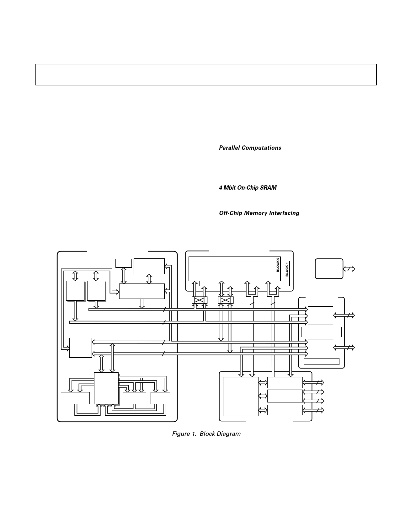
Parallel Computations
Single-Cycle Multiply and ALU Operations in Parallel
with Dual Memory Read/Writes and Instruction Fetch
Multiply with Add and Subtract for Accelerated FFT
Butterfly Computation
4 Mbit On-Chip SRAM
Dual-Ported for Independent Access by Core Processor
and DMA
Off-Chip Memory Interfacing
4 Gigawords Addressable
Programmable Wait State Generation, Page-Mode
DRAM Support
CORE PROCESSOR
TIMER
INSTRUCTION
CACHE
32 ؋ 48-BIT
DAG1 DAG2
8 ؋ 4 ؋ 32 8 ؋ 4 ؋ 24
PROGRAM
SEQUENCER
PM ADDRESS BUS
24
DM ADDRESS BUS
32
BUS
CONNECT
(PX)
PM DATA BUS
48
DM DATA BUS 40/32
DUAL-PORTED SRAM
TWO INDEPENDENT
DUAL-PORTED BLOCKS
PROCESSOR PORT
ADDR
DATA
I/O PORT
DATA
ADDR
ADDR
DATA
DATA
ADDR
IOD IOA
48 17
JTAG
TEST &
EMULATION
7
EXTERNAL
PORT
ADDR BUS
MUX
32
MULTIPROCESSOR
INTERFACE
DATA BUS
MUX
48
HOST PORT
MULTIPLIER
DATA
REGISTER
FILE
16 ؋ 40-BIT
BARREL
SHIFTER
ALU
IOP
REGISTERS
(MEMORY MAPPED)
CONTROL,
STATUS &
DATA BUFFERS
DMA
CONTROLLER
SERIAL PORTS
(2)
LINK PORTS
(6)
I/O PROCESSOR
Figure 1. Block Diagram
4
6
6
36
SHARC is a registered trademark of Analog Devices, Inc.
REV. D
Information furnished by Analog Devices is believed to be accurate and
reliable. However, no responsibility is assumed by Analog Devices for its
use, nor for any infringements of patents or other rights of third parties
which may result from its use. No license is granted by implication or
otherwise under any patent or patent rights of Analog Devices.
One Technology Way, P.O. Box 9106, Norwood, MA 02062-9106, U.S.A.
Tel: 781/329-4700
World Wide Web Site: http://www.analog.com
Fax: 781/326-8703
© Analog Devices, Inc., 2000
1 page 
ADSP-21060/ADSP-21060L
Serial Ports
The ADSP-2106x features two synchronous serial ports that
provide an inexpensive interface to a wide variety of digital and
mixed-signal peripheral devices. The serial ports can operate at
the full clock rate of the processor, providing each with a maxi-
mum data rate of 40 Mbit/s. Independent transmit and receive
functions provide greater flexibility for serial communications.
Serial port data can be automatically transferred to and from
on-chip memory via DMA. Each of the serial ports offers TDM
multichannel mode.
The serial ports can operate with little-endian or big-endian
transmission formats, with word lengths selectable from 3 bits to
32 bits. They offer selectable synchronization and transmit
modes as well as optional µ-law or A-law companding. Serial
port clocks and frame syncs can be internally or externally
generated.
Multiprocessing
The ADSP-2106x offers powerful features tailored to multi-
processing DSP systems. The unified address space (see
Figure 4) allows direct interprocessor accesses of each ADSP-
2106x’s internal memory. Distributed bus arbitration logic is
included on-chip for simple, glueless connection of systems
containing up to six ADSP-2106xs and a host processor. Master
processor changeover incurs only one cycle of overhead. Bus
arbitration is selectable as either fixed or rotating priority. Bus lock
allows indivisible read-modify-write sequences for semaphores. A
vector interrupt is provided for interprocessor commands. Maxi-
mum throughput for interprocessor data transfer is 240 Mbytes/s
over the link ports or external port. Broadcast writes allow simulta-
neous transmission of data to all ADSP-2106xs and can be used
to implement reflective semaphores.
Link Ports
The ADSP-2106x features six 4-bit link ports that provide addi-
tional I/O capabilities. The link ports can be clocked twice per
cycle, allowing each to transfer eight bits per cycle. Link port
I/O is especially useful for point-to-point interprocessor commu-
nication in multiprocessing systems.
The link ports can operate independently and simultaneously,
with a maximum data throughput of 240 Mbytes/s. Link port
data is packed into 32- or 48-bit words, and can be directly read
by the core processor or DMA-transferred to on-chip memory.
Each link port has its own double-buffered input and output
registers. Clock/acknowledge handshaking controls link port
transfers. Transfers are programmable as either transmit or
receive.
Program Booting
The internal memory of the ADSP-2106x can be booted at
system power-up from either an 8-bit EPROM, a host proces-
sor, or through one of the link ports. Selection of the boot
source is controlled by the BMS (Boot Memory Select),
EBOOT (EPROM Boot), and LBOOT (Link/Host Boot) pins.
32-bit and 16-bit host processors can be used for booting.
REV. D
–5–
5 Page 
ADSP-21060/ADSP-21060L
TARGET BOARD CONNECTOR FOR EZ-ICE PROBE
The ADSP-2106x EZ-ICE Emulator uses the IEEE 1149.1
JTAG test access port of the ADSP-2106x to monitor and control
the target board processor during emulation. The EZ-ICE probe
requires the ADSP-2106x’s CLKIN, TMS, TCK, TRST, TDI,
TDO, EMU, and GND signals be made accessible on the target
system via a 14-pin connector (a 2 row × 7 pin strip header) such
as that shown in Figure 5. The EZ-ICE probe plugs directly onto
this connector for chip-on-board emulation. You must add this
connector to your target board design if you intend to use the
ADSP-2106x EZ-ICE. The total trace length between the EZ-
ICE connector and the furthest device sharing the EZ-ICE
JTAG pins should be limited to 15 inches maximum for guaran-
teed operation. This length restriction must include EZ-ICE
JTAG signals that are routed to one or more ADSP-2106x
devices, or a combination of ADSP-2106x devices and other
JTAG devices on the chain.
GND
KEY (NO PIN)
BTMS
BTCK
BTRST
BTDI
GND
1
3
5
7
9
9
11
13
2
EMU
4
CLKIN (OPTIONAL)
6
TMS
8
TCK
10
TRST
12
TDI
14
TDO
TOP VIEW
Figure 5. Target Board Connector For ADSP-2106x EZ-ICE
Emulator (Jumpers in Place)
The 14-pin, 2-row pin strip header is keyed at the Pin 3 location —
Pin 3 must be removed from the header. The pins must be
0.025 inch square and at least 0.20 inch in length. Pin spacing
should be 0.1 × 0.1 inches. Pin strip headers are available from
vendors such as 3M, McKenzie and Samtec.
The BTMS, BTCK, BTRST and BTDI signals are provided so
the test access port can also be used for board-level testing.
When the connector is not being used for emulation, place
jumpers between the Bxxx pins and the xxx pins. If the test
access port will not be used for board testing, tie BTRST to GND
and tie or pull BTCK up to VDD. The TRST pin must be
asserted after power-up (through BTRST on the connector) or
held low for proper operation of the ADSP-2106x. None of the
Bxxx pins (Pins 5, 7, 9, 11) are connected on the EZ-ICE probe.
The JTAG signals are terminated on the EZ-ICE probe as
follows:
Signal Termination
TMS Driven through 22 Ω Resistor (16 mA Driver)
TCK Driven at 10 MHz through 22 Ω Resistor (16 mA
Driver)
TRST* Active Low Driven through 22 Ω Resistor (16 mA
Driver) (Pulled Up by On-Chip 20 kΩ Resistor)
TDI Driven by 22 Ω Resistor (16 mA Driver)
TDO One TTL Load, Split Termination (160/220)
CLKIN One TTL Load, Split Termination (160/220)
EMU Active Low 4.7 kΩ Pull-Up Resistor, One TTL Load
(Open-Drain Output from the DSP)
*TRST is driven low until the EZ-ICE probe is turned on by the emulator at
software start-up. After software start-up, TRST is driven high.
Figure 6 shows JTAG scan path connections for systems that
contain multiple ADSP-2106x processors.
ADSP-2106x
#1
JTAG
DEVICE
(OPTIONAL)
ADSP-2106x
n
OTHER
JTAG
CONTROLLER
TDI
EZ-ICE
JTAG
CONNECTOR
TCK
TMS
EMU
TRST
TDO
CLKIN
TDI TDO
OPTIONAL
TDI
TDO
TDI TDO
Figure 6. JTAG Scan Path Connections for Multiple ADSP-2106x Systems
REV. D
–11–
11 Page | ||
| Páginas | Total 30 Páginas | |
| PDF Descargar | [ Datasheet ADSP-21060LKB-160.PDF ] | |
Hoja de datos destacado
| Número de pieza | Descripción | Fabricantes |
| ADSP-21060LKB-160 | ADSP-2106x SHARC DSP Microcomputer Family | Analog Devices |
| Número de pieza | Descripción | Fabricantes |
| SLA6805M | High Voltage 3 phase Motor Driver IC. |
Sanken |
| SDC1742 | 12- and 14-Bit Hybrid Synchro / Resolver-to-Digital Converters. |
Analog Devices |
|
DataSheet.es es una pagina web que funciona como un repositorio de manuales o hoja de datos de muchos de los productos más populares, |
| DataSheet.es | 2020 | Privacy Policy | Contacto | Buscar |