|
|
|
PDF ADV7185 Data sheet ( Hoja de datos )
| Número de pieza | ADV7185 | |
| Descripción | Professional NTSC/PAL Video Decoder with 10-Bit CCIR656 Output | |
| Fabricantes | Analog Devices | |
| Logotipo | ||
Hay una vista previa y un enlace de descarga de ADV7185 (archivo pdf) en la parte inferior de esta página. Total 30 Páginas | ||
|
No Preview Available !
a
Professional NTSC/PAL Video Decoder
with 10-Bit CCIR656 Output
ADV7185
FEATURES
Analog Video to Digital YCrCb Video Decoder:
NTSC-(M/N), PAL-(B/D/G/H/I/M/N)
ADV®7185 Integrates Two 12-Bit ADCs
Clocked from a Single 27 MHz Crystal
Dual Video Clocking Schemes:
Line-Locked Clock Compatible (LLC)
Adaptive Digital Line Length Tracking (ADLLT™)
3-Line Chroma Comb Filter
Real-Time Clock and Status Information Output
Integrated AGC (Automatic Gain Control) and Clamping
Multiple Programmable Analog Input Formats:
CVBS (Composite Video)
SVHS (Y/C)
YCrCb Component (VESA, MII, SMPTE, and BetaCam)
6 Analog Input Video Channels
Real-Time Horizontal and Vertical Scaling
Automatic NTSC/PAL Identification
Differential Mode Video Input
Digital Output Formats (20-Bit Wide Bus):
YCrCb (4:2:2 or 4:1:1)
CCIR601/CCIR656 8-Bit or Extended 10-Bit
0.5 V to 2.0 V p-p Input Range
Differential Gain, 0.4% Typ
Differential Phase, 0.6o Typ
Programmable Video Controls:
Peak White/Hue/Brightness/Saturation/Contrast
CCIR/Square/4 FSC Pixel Operation
APPLICATIONS
Projectors
Digital TVs
DVD-RAM Recorders and Players
PDP Displays
Video Decoders
Hybrid Analog/Digital Set-Top Boxes
Professional Equipment
(continued on page 9)
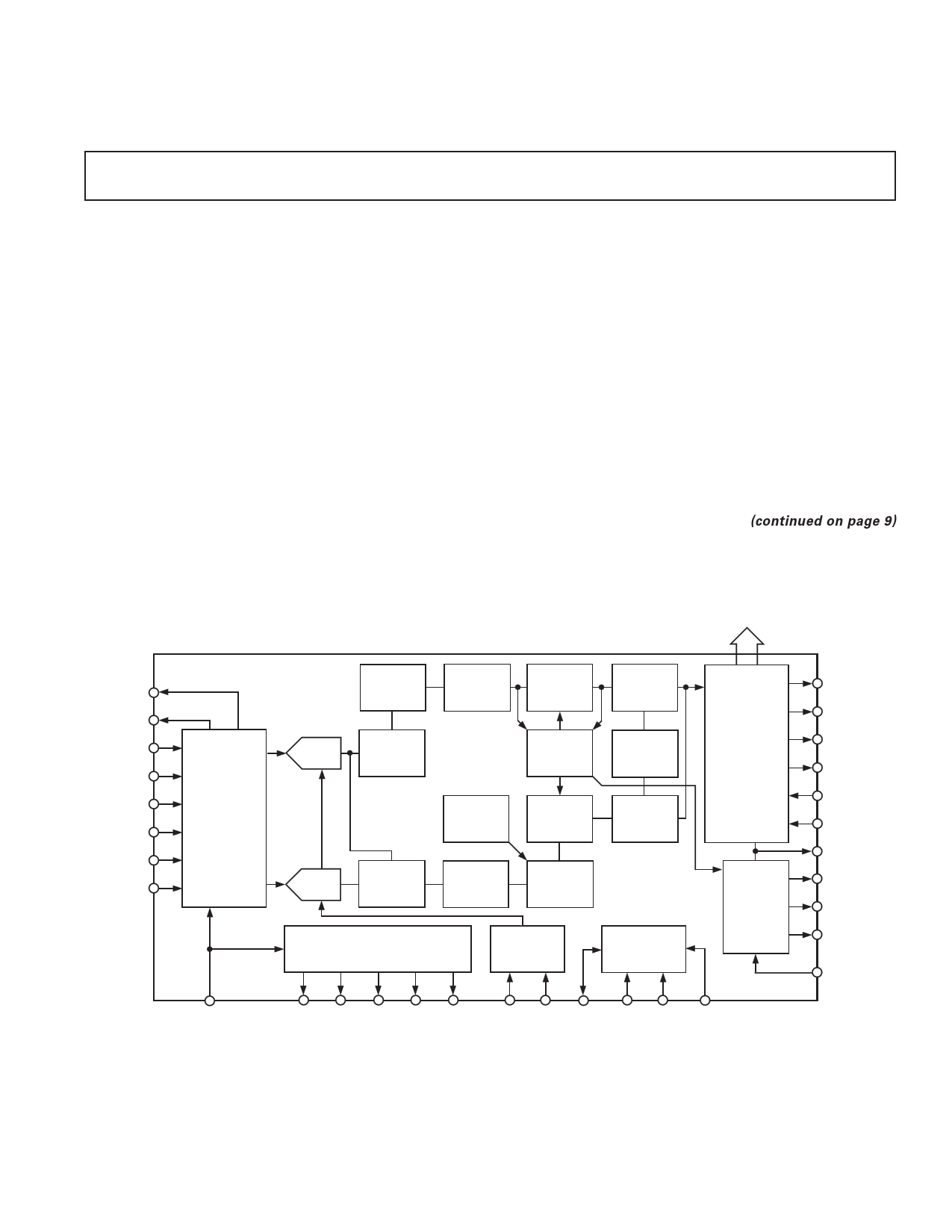
FUNCTIONAL BLOCK DIAGRAM
P19–P0
PIXEL
O/P PORT
ADV7185
ISO
REFOUT
AIN1
AIN2
AIN3
AIN4
AIN5
AIN6
ANALOG I/P
MULTIPLEXING
AUTOMATIC
GAIN
CONTROL
(AGC )
CLAMP AND
DC RESTORE
SHAPING
AND
NOTCH LPF
12-BIT
ADC
LUMA
ANTIALIAS
LPF
27MHz
12-BIT
ADC
SWITCH
VIDEO TIMING AND
CONTROL BLOCK
PEAKING
HPF/LPF
RESAMPLING
AND
HORIZONTAL
SCALING
LUMA
DELAY
BLOCK
SYNC
DETECTION
2H LINE
MEMORY
SUB-
CARRIER
RECOVERY
DTO
RESAMPLING
AND
HORIZONTAL
SCALING
CHROMA
COMB
FILTER
CHROMA
ANTIALIAS
LPF
SHAPING
LPF
27MHz XTAL
OSCILLATOR
BLOCK
I2C-COMPATIBLE
INTERFACE PORT
FIFO CONTROL
BLOCK
AND
PIXEL
OUTPUT
FORMATTER
LLC
SYNTHESIS
WITH LINE-
LOCKED
OUTPUT
CLOCK
AFF
HFF/QCLK
AEF
DV
RD
OE
GL/CLKIN
LLC1
LLC2
LLCREF
ELPF
PWRDN
HSYNC FIELD VSYNC HREF VREF
CLOCK CLOCK RESET SDATA SCLOCK ALSB
ADLLT is a trademark and ADV is a registered trademark of Analog Devices, Inc.
REV. 0
Information furnished by Analog Devices is believed to be accurate and
reliable. However, no responsibility is assumed by Analog Devices for its
use, nor for any infringements of patents or other rights of third parties that
may result from its use. No license is granted by implication or otherwise
under any patent or patent rights of Analog Devices.
One Technology Way, P.O. Box 9106, Norwood, MA 02062-9106, U.S.A.
Tel: 781/329-4700
www.analog.com
Fax: 781/326-8703
© Analog Devices, Inc., 2002
1 page 
SDATA
SCLOCK
t3 t6
t3
t1 t5
t2 t7
t4
Figure 1. MPU Port Timing Diagram
t8
ADV7185
LLC1
LLCREF
t9
t10
t11
t12
t13
LLC2
t14 t15
OUTPUTS P0–P19, HREF, VREF,
VSYNC, HSYNC, FIELD, DV
t17
t16
Figure 2. LLC Clock, Pixel Port, and Control Outputs Timing Diagram
CLKIN
t18
OUTPUTS P0–P19, HREF, VREF,
VSYNC, HSYNC, FIELD, DV
t20
t19
Figure 3. Pixel Port and Control Outputs in CAPI and SCAPI Mode Timing Diagram
OE
OUTPUTS P0–P19, HS, VS, VREF,
HREF, FIELD, DV
t21
t23
t22
Figure 4. OE Timing Diagram
REV. 0
–5–
5 Page 
LUMINANCE PROCESSING
Figure 7 shows the luminance data path. The 12-bit data from
the Y ADC is applied to an antialiasing low-pass filter that is
designed to band-limit the input video signal such that aliasing
does not occur. This filter dramatically reduces the design on an
external analog antialiasing filter; this filter need only remove
components in the input video signal above 22 MHz. The data
then passes through a shaping or notch filter.
When in CVBS mode, a notch filter must be used to remove the
unwanted chrominance data that lies around the subcarrier
frequency. A wide variety of programmable notch filters for
both PAL and NTSC are available. The YSFM[4:0] control the
selection of these filters; refer to Figures 8 and 9 for plots of
these filters. If S-video or component mode is selected a notch
filter is not required. The ADV7185 offers 18 possible shaping
filters (SVHS1-18) with a range of low-pass filter responses
from 0.5 MHz up to 5.75 MHz. The YSFM[4:0] control the
selection of these filters. Please refer to Figures 8 through 16 for
filter plots.
The next stage in the luminance processing path is a peaking
filter. This filter offers a sharpness function on the luminance
path. The degree of sharpness can be selected using YPM[2:0].
If no sharpness is required, this filter can be bypassed.
The luminance data is then passed through a resampler to correct
for line length variations in the input video. This resampler is
designed to always output 720 pixels per line for standard PAL or
NTSC. The resampler used on the ADV7185 is of very high quality
as it uses 128 phases to resample the video, giving 1/128 pixel
resolution. The resampler is controlled by a sync detection block
that calculates line length variations on the input video.
The final stage in the luminance path, before it is applied to an
output formatter block, is a 2-line delay store that is used to
compensate for delays in the chroma datapath when chroma
comb filter is selected.
ADC DATA
ANTI-
ALIASING
LPF
SYNC
DETECTION
SHAPING
AND
NOTCH
FILTER
PEAKING
FILTER
RESAMPLE
Y
DELAY
LINE
STORES
Figure 7. Luminance Processing Path
ADV7185
0
–10 SVHS1
SVHS2
SVHS3
SVHS4
SVHS17
SVHS18
–20 SVHS5
SVHS6
SVHS7
SVHS8
–30 SVHS9
SVHS10
SVHS11
SVHS12
–40 SVHS13
SVHS14
SVHS15
SVHS16
–50
–60
0
1
23
45
6
FREQUENCY – MHz
7
8
Figure 8. Luminance SVHS1–SVHS18 Shaping
Filter Responses
1.0
0.8
0.6
0.4
0.2
0
–0.2
–0.4
–0.6
–0.8
–1.00 1 2 3 4 5 6
FREQUENCY – MHz
Figure 9. Luminance SVHS1–SVHS18 Shaping
Filter Responses (Close-Up)
0
NTSC WN1
NTSC WN2
NTSC WN3
–10 NTSC NN1
NTSC NN2
NTSC NN3
–20
–30
–40
NTSC WN2
NTSC NN3
NTSC WN1
NTSC NN2
NTSC NN1
NTSC WN3
–50
–60
0
1
23
45
6
FREQUENCY – MHz
7
8
Figure 10. Luminance NTSC Narrow/Wide Notch
Shaping Filter
REV. 0
–11–
11 Page | ||
| Páginas | Total 30 Páginas | |
| PDF Descargar | [ Datasheet ADV7185.PDF ] | |
Hoja de datos destacado
| Número de pieza | Descripción | Fabricantes |
| ADV7180 | 4 x Oversampling SDTV Video Decoder | Analog Devices |
| ADV7181 | Multiformat SDTV Video Decoder | Analog Devices |
| ADV7181B | Multiformat SDTV Video Decoder | Analog Devices |
| ADV7183A | Multiformat SDTV Video Decoder | Analog Devices |
| Número de pieza | Descripción | Fabricantes |
| SLA6805M | High Voltage 3 phase Motor Driver IC. |
Sanken |
| SDC1742 | 12- and 14-Bit Hybrid Synchro / Resolver-to-Digital Converters. |
Analog Devices |
|
DataSheet.es es una pagina web que funciona como un repositorio de manuales o hoja de datos de muchos de los productos más populares, |
| DataSheet.es | 2020 | Privacy Policy | Contacto | Buscar |