|
|
PDF ADV7181 Data sheet ( Hoja de datos )
| Número de pieza | ADV7181 | |
| Descripción | Multiformat SDTV Video Decoder | |
| Fabricantes | Analog Devices | |
| Logotipo |  |
|
Hay una vista previa y un enlace de descarga de ADV7181 (archivo pdf) en la parte inferior de esta página. Total 30 Páginas | ||
|
No Preview Available !
FEATURES
Multiformat video decoder supports NTSC-(J, M, 4.43),
PAL-(B/D/G/H/I/M/N), SECAM
Integrates three 54 MHz, 9-bit ADCs
Clocked from a single 27 MHz crystal
Line-locked clock-compatible (LLC)
Adaptive Digital Line Length Tracking (ADLLT™)
5-line adaptive comb filters
Proprietary architecture for locking to weak, noisy, and
unstable video sources such as VCRs and tuners
Subcarrier frequency lock and status information output
Integrated AGC with adaptive peak white mode
Macrovision® copy protection detection
CTI (chroma transient improvement)
DNR (digital noise reduction)
Multiple programmable analog input formats:
CVBS (composite video)
S-Video (Y/C)
YPrPb component (VESA, MII, SMPTE, and Betacam)
6 analog video input channels
Automatic NTSC/PAL/SECAM identification
Digital output formats (8-bit or16-bit):
ITU-R BT.656 YCrCb 4:2:2 output + HS, VS, and FIELD
0.5 V to 1.6 V analog signal input range
Differential gain: 0.6% typ
GENERAL DESCRIPTION
The ADV7181 integrated video decoder automatically detects
and converts a standard analog baseband television signal
compatible with worldwide standards NTSC, PAL, and SECAM
into 4:2:2 component video data compatible with 16-/8-bit
CCIR601/CCIR656.
The advanced, highly flexible digital output interface enables
performance video decoding and conversion in line-locked
clock-based systems. This makes the device ideally suited for a
broad range of applications with diverse analog video charac-
teristics, including tape-based sources, broadcast sources,
security/surveillance cameras, and professional systems.
The six analog input channels accept standard composite,
S-Video, YPrPb video signals in an extensive number of
combinations. AGC and clamp restore circuitry allow an input
video signal peak-to-peak range of 0.5 V up to 1.6 V.
Alternatively, these can be bypassed for manual settings.
Multiformat SDTV Video Decoder
ADV7181
Differential phase: 0.6° typ
Programmable video controls:
Peak-white/hue/brightness/saturation/contrast
Integrated on-chip video timing generator
Free run mode (generates stable video ouput with no I/P)
VBI decode support for
Close captioning, WSS, CGMS, EDTV, Gemstar® 1×/2×
Power-down mode
2-wire serial MPU interface (I2C®-compatible)
3.3 V analog, 1.8 V digital core; 3.3 V IO supply
Temperature grade: –40°C to +85°C
64-lead LQFP Pb-free package
APPLICATIONS
DVD recorders
PC video
HDD-based PVRs/DVDRs
LCD TVs
Set-top boxes
Security systems
Digital televisions
Portable video devices
Automotive entertainment
AVR receiver
The fixed 54 MHz clocking of the ADCs and datapath for all
modes allow very precise, accurate sampling and digital
filtering. The line-locked clock output allows the output data
rate, timing signals, and output clock signals to be synchronous,
asynchronous, or line locked even with ±5% line length
variation. The output control signals allow glueless interface
connections in almost any application. The ADV7181 modes
are set up over a 2-wire, serial, bidirectional port (I2C-
compatible).
The ADV7181 is fabricated in a 3.3 V CMOS process. Its
monolithic CMOS construction ensures greater functionality
with lower power dissipation.
The ADV7181 is packaged in a small 64-lead LFCSP and LQFP
and Pb-free packages.
Rev. B
Information furnished by Analog Devices is believed to be accurate and reliable.
However, no responsibility is assumed by Analog Devices for its use, nor for any
infringements of patents or other rights of third parties that may result from its use.
Specifications subject to change without notice. No license is granted by implication
or otherwise under any patent or patent rights of Analog Devices. Trademarks and
registered trademarks are the property of their respective owners.
One Technology Way, P.O. Box 9106, Norwood, MA 02062-9106, U.S.A.
Tel: 781.329.4700
Fax: 781.461.3113
www.analog.com
© 2005 Analog Devices, Inc. All rights reserved.
1 page 
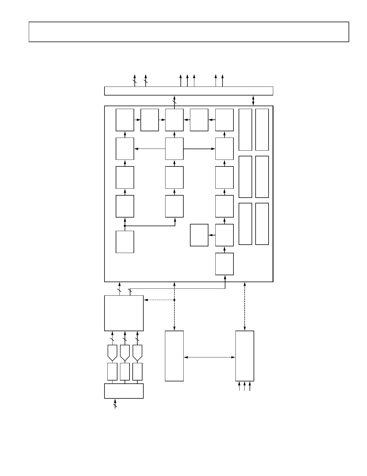
FUNCTIONAL BLOCK DIAGRAM
ADV7181
Figure 1.
Rev. B | Page 5 of 104
5 Page 
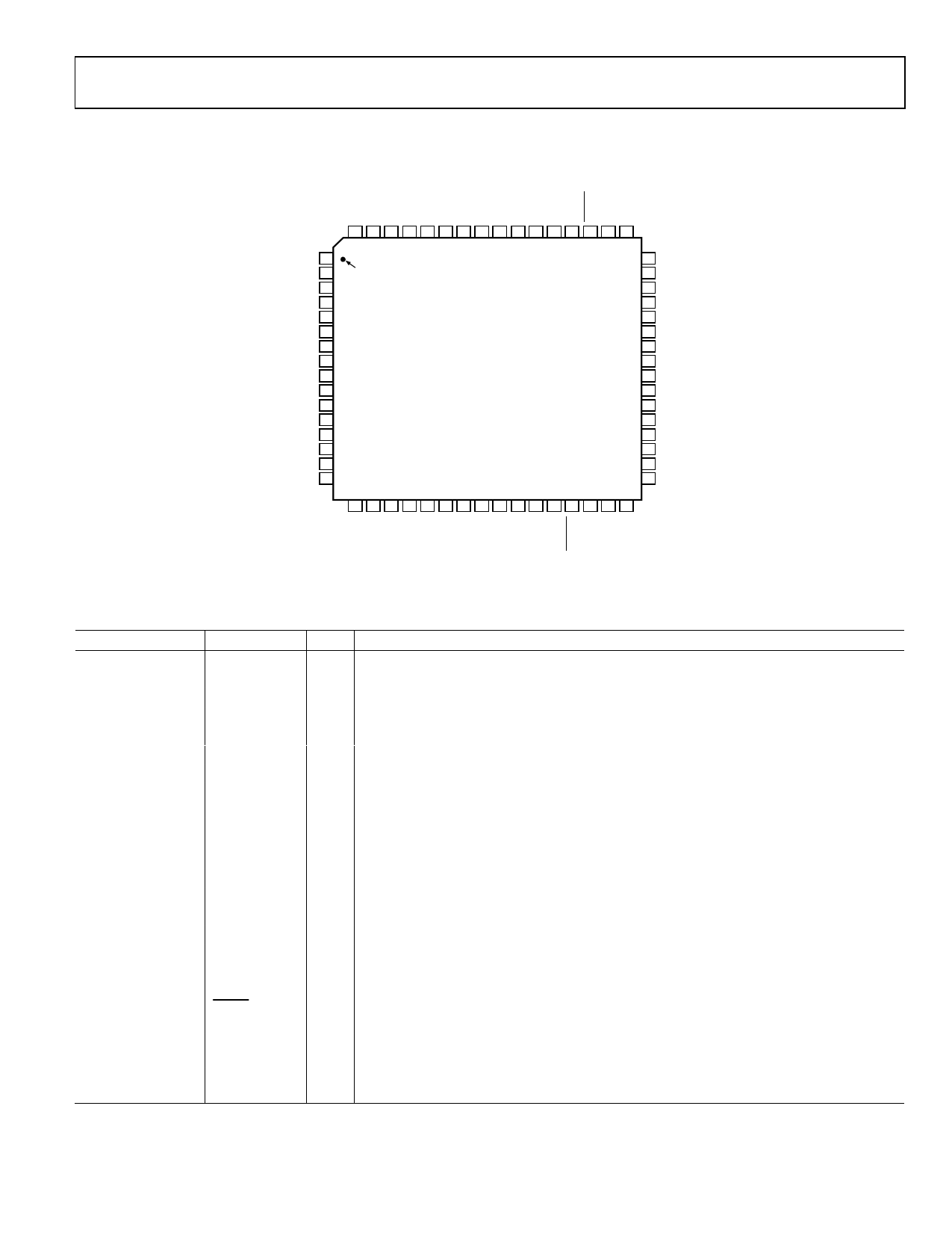
PIN CONFIGURATION AND FUNCTION DESCRIPTIONS
ADV7181
64 63 62 61 60 59 58 57 56 55 54 53 52 51 50 49
NC 1
HS 2
DGND 3
DVDDIO 4
P11 5
P10 6
P9 7
P8 8
SFL 9
DGND 10
DVDDIO 11
NC 12
NC 13
P7 14
P6 15
P5 16
PIN 1
INDICATOR
ADV7181
TOP VIEW
(Not to Scale)
48 AIN5
47 AIN4
46 AIN3
45 AGND
44 CAPC2
43 AGND
42 CML
41 REFOUT
40 AVDD
39 CAPY2
38 CAPY1
37 AGND
36 AIN2
35 AIN1
34 DGND
33 NC
17 18 19 20 21 22 23 24 25 26 27 28 29 30 31 32
NC = NO CONNECT
Figure 4. 64-Lead LFCSP/LQFP Pin Configuration
Table 7. Pin Function Descriptions
Pin No.
Mnemonic
3, 10, 24, 34, 57
DGND
32, 37, 43, 45
AGND
4, 11 DVDDIO
23, 58
DVDD
40 AVDD
31 PVDD
35, 36, 46–49
AIN1–AIN6
1, 12, 13, 27, 28, 33, NC
50, 55, 56
26, 25, 19, 18, 17, P0–P15
16, 15, 14, 8, 7, 6, 5,
62, 61, 60, 59
2 HS
64 VS
63 FIELD
53 SDA
54 SCLK
52 ALSB
51 RESET
20 LLC
22 XTAL
Type
G
G
P
P
P
P
I
O
O
O
O
I/O
I
I
I
O
I
Function
Digital Ground.
Analog Ground.
Digital I/O Supply Voltage (3.3 V).
Digital Core Supply Voltage (1.8 V).
Analog Supply Voltage (3.3 V).
PLL Supply Voltage (1.8 V).
Analog Video Input Channels.
No Connect Pins.
Video Pixel Output Port.
Horizontal Synchronization Output Signal.
Vertical Synchronization Output Signal.
Field Synchronization Output Signal.
I2C Port Serial Data Input/Output Pin.
I2C Port Serial Clock Input (Max Clock Rate of 400 kHz).
This pin selects the I2C address for the ADV7181. ALSB set to a Logic 0 sets the address for a
write as 0x40; for ALSB set to a logic high, the address selected is 0x42.
System Reset Input, Active Low. A minimum low reset pulse width of 5 ms is required to
reset the ADV7181 circuitry.
This is a line-locked output clock for the pixel data output by the ADV7181. Nominally
27 MHz, but varies up or down according to video line length.
This is the input pin for the 27 MHz crystal, or can be overdriven by an external 3.3 V,
27 MHz clock oscillator source. In crystal mode, the crystal must be a fundamental crystal.
Rev. B | Page 11 of 104
11 Page | ||
| Páginas | Total 30 Páginas | |
| PDF Descargar | [ Datasheet ADV7181.PDF ] | |
Hoja de datos destacado
| Número de pieza | Descripción | Fabricantes |
| ADV7180 | 4 x Oversampling SDTV Video Decoder | Analog Devices |
| ADV7181 | Multiformat SDTV Video Decoder | Analog Devices |
| ADV7181B | Multiformat SDTV Video Decoder | Analog Devices |
| ADV7183A | Multiformat SDTV Video Decoder | Analog Devices |
| Número de pieza | Descripción | Fabricantes |
| SLA6805M | High Voltage 3 phase Motor Driver IC. |
Sanken |
| SDC1742 | 12- and 14-Bit Hybrid Synchro / Resolver-to-Digital Converters. |
Analog Devices |
|
DataSheet.es es una pagina web que funciona como un repositorio de manuales o hoja de datos de muchos de los productos más populares, |
| DataSheet.es | 2020 | Privacy Policy | Contacto | Buscar |
