|
|
|
PDF BFR31LT1 Data sheet ( Hoja de datos )
| Número de pieza | BFR31LT1 | |
| Descripción | JFET Amplifiers(N-Channel) | |
| Fabricantes | Motorola Inc | |
| Logotipo | ||
Hay una vista previa y un enlace de descarga de BFR31LT1 (archivo pdf) en la parte inferior de esta página. Total 6 Páginas | ||
|
No Preview Available !
MOTOROLA
SEMICONDUCTOR TECHNICAL DATA
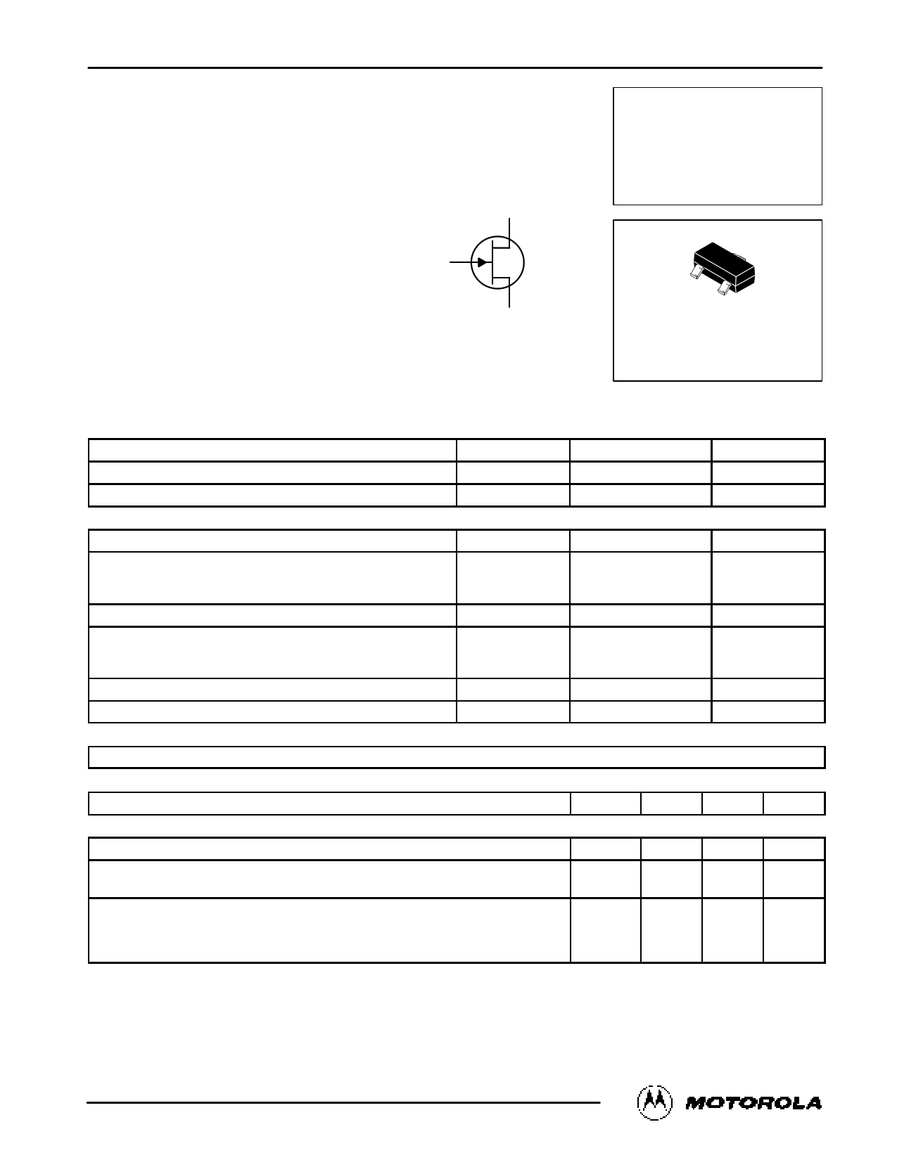
JFET Amplifiers
N – Channel
3
GATE
2 SOURCE
1 DRAIN
Order this document
by BFR30LT1/D
BFR30LT1
BFR31LT1
3
1
2
CASE 318 – 08, STYLE 10
SOT– 23 (TO – 236AB)
MAXIMUM RATINGS
Rating
Symbol
Value
Drain – Source Voltage
Gate – Source Voltage
THERMAL CHARACTERISTICS
VDS
VGS
25
25
Characteristic
Total Device Dissipation(1)
TA = 25°C
Derate above 25°C
Symbol
PD
Max
225
1.8
Thermal Resistance Junction to Ambient
Total Device Dissipation
Alumina Substrate,(2) TA = 25°C
Derate above 25°C
RqJA
PD
556
300
2.4
Thermal Resistance Junction to Ambient
Junction and Storage Temperature
DEVICE MARKING
RqJA
TJ, Tstg
417
– 55 to +150
BFR30LT1 = M1; BFR31LT1 = M2
ELECTRICAL CHARACTERISTICS (TA = 25°C unless otherwise noted)
Characteristic
Symbol
Min
OFF CHARACTERISTICS
Gate Reverse Current
Gate Source Cutoff Voltage
(VGS = 10 Vdc, VDS = 0)
(ID = 0.5 nAdc, VDS = 10 Vdc)
BFR30
BFR31
IGSS
VGS(OFF)
—
—
—
Gate Source Voltage
(ID = 1.0 mAdc, VDS = 10 Vdc)
(ID = 50 mAdc, VDS = 10 Vdc)
BFR30
BFR31
BFR30
BFR31
VGS
– 0.7
—
—
—
1. Device mounted on FR4 glass epoxy printed circuit board using the recommended footprint.
2. Alumina = 0.4 x 0.3 x 0.024 in. 99.5% alumina.
Unit
Vdc
Vdc
Unit
mW
mW/°C
°C/W
mW
mW/°C
°C/W
°C
Max Unit
0.2
5.0
2.5
– 3.0
– 1.3
– 4.0
– 2.0
nAdc
Vdc
Vdc
Thermal Clad is a registered trademark of the Berquist Company.
©MMotootorroollaa, SInmc. 1a9ll9–6Signal Transistors, FETs and Diodes Device Data
1
1 page 
BFR30LT1 BFR31LT1
INFORMATION FOR USING THE SOT–23 SURFACE MOUNT PACKAGE
MINIMUM RECOMMENDED FOOTPRINT FOR SURFACE MOUNTED APPLICATIONS
Surface mount board layout is a critical portion of the total
design. The footprint for the semiconductor packages must
be the correct size to insure proper solder connection
interface between the board and the package. With the
correct pad geometry, the packages will self align when
subjected to a solder reflow process.
0.037
0.95
0.037
0.95
0.035
0.9
0.079
2.0
0.031
0.8
SOT–23
inches
mm
SOT–23 POWER DISSIPATION
The power dissipation of the SOT–23 is a function of the
drain pad size. This can vary from the minimum pad size for
soldering to a pad size given for maximum power dissipation.
Power dissipation for a surface mount device is determined
by TJ(max), the maximum rated junction temperature of the
die, RθJA, the thermal resistance from the device junction to
ambient, and the operating temperature, TA. Using the
values provided on the data sheet for the SOT–23 package,
PD can be calculated as follows:
PD =
TJ(max) – TA
RθJA
The values for the equation are found in the maximum
ratings table on the data sheet. Substituting these values into
the equation for an ambient temperature TA of 25°C, one can
calculate the power dissipation of the device which in this
case is 225 milliwatts.
PD =
150°C – 25°C
556°C/W
= 225 milliwatts
The 556°C/W for the SOT–23 package assumes the use
of the recommended footprint on a glass epoxy printed circuit
board to achieve a power dissipation of 225 milliwatts. There
are other alternatives to achieving higher power dissipation
from the SOT–23 package. Another alternative would be to
use a ceramic substrate or an aluminum core board such as
Thermal Clad™. Using a board material such as Thermal
Clad, an aluminum core board, the power dissipation can be
doubled using the same footprint.
SOLDERING PRECAUTIONS
The melting temperature of solder is higher than the rated
temperature of the device. When the entire device is heated
to a high temperature, failure to complete soldering within a
short time could result in device failure. Therefore, the
following items should always be observed in order to
minimize the thermal stress to which the devices are
subjected.
• Always preheat the device.
• The delta temperature between the preheat and
soldering should be 100°C or less.*
• When preheating and soldering, the temperature of the
leads and the case must not exceed the maximum
temperature ratings as shown on the data sheet. When
using infrared heating with the reflow soldering method,
the difference shall be a maximum of 10°C.
• The soldering temperature and time shall not exceed
260°C for more than 10 seconds.
• When shifting from preheating to soldering, the
maximum temperature gradient shall be 5°C or less.
• After soldering has been completed, the device should
be allowed to cool naturally for at least three minutes.
Gradual cooling should be used as the use of forced
cooling will increase the temperature gradient and result
in latent failure due to mechanical stress.
• Mechanical stress or shock should not be applied during
cooling.
* Soldering a device without preheating can cause excessive
thermal shock and stress which can result in damage to the
device.
Motorola Small–Signal Transistors, FETs and Diodes Device Data
5
5 Page | ||
| Páginas | Total 6 Páginas | |
| PDF Descargar | [ Datasheet BFR31LT1.PDF ] | |
Hoja de datos destacado
| Número de pieza | Descripción | Fabricantes |
| BFR31LT1 | JFET Amplifiers(N-Channel) | Motorola Inc |
| BFR31LT1 | JFET Amplifiers | ON Semiconductor |
| Número de pieza | Descripción | Fabricantes |
| SLA6805M | High Voltage 3 phase Motor Driver IC. |
Sanken |
| SDC1742 | 12- and 14-Bit Hybrid Synchro / Resolver-to-Digital Converters. |
Analog Devices |
|
DataSheet.es es una pagina web que funciona como un repositorio de manuales o hoja de datos de muchos de los productos más populares, |
| DataSheet.es | 2020 | Privacy Policy | Contacto | Buscar |