|
|
|
PDF MT5VDDT1672A Data sheet ( Hoja de datos )
| Número de pieza | MT5VDDT1672A | |
| Descripción | 128MB DDR SDRAM UDIMM | |
| Fabricantes | Micron | |
| Logotipo | ||
Hay una vista previa y un enlace de descarga de MT5VDDT1672A (archivo pdf) en la parte inferior de esta página. Total 12 Páginas | ||
|
No Preview Available !
64MB, 128MB, 256MB (x72, ECC, SR) 184-Pin DDR SDRAM UDIMM
Features
DDR SDRAM UDIMM
MT5VDDT872A – 64MB1
MT5VDDT1672A – 128MB2
MT5VDDT3272A – 256MB2
For component data sheets, refer to Micron’s Web site: www.micron.com
Features
• 184-pin, unbuffered dual in-line memory module
(UDIMM)
• Fast data transfer rates: PC2100, PC2700, or PC3200
• 64MB (8 Meg x 72), 128MB (16 Meg x 72), and
256MB (32 Meg x 72)
• Supports ECC error detection and correction
• VDD = VDDQ = +2.5V
(-40B: VDD = VDDQ = +2.6V)
• VDDSPD = +2.3V to +3.6V
• 2.5V I/O (SSTL_2-compatible)
• Internal, pipelined double data rate (DDR)
2n-prefetch architecture
• Bidirectional data strobe (DQS) transmitted/
received with data—that is, source-synchronous
data capture
• Differential clock inputs (CK and CK#)
• Multiple internal device banks for concurrent
operation
• Single rank
• Selectable burst lengths (BL): 2, 4, or 8
• Auto precharge option
• Auto refresh and self refresh modes:
64MB = 15.625µs and 128MB, 256MB = 7.8125µs
maximum average periodic refresh interval
• Serial presence-detect (SPD) with EEPROM
• Selectable CAS latency (CL) for maximum
compatibility
• Gold edge contacts
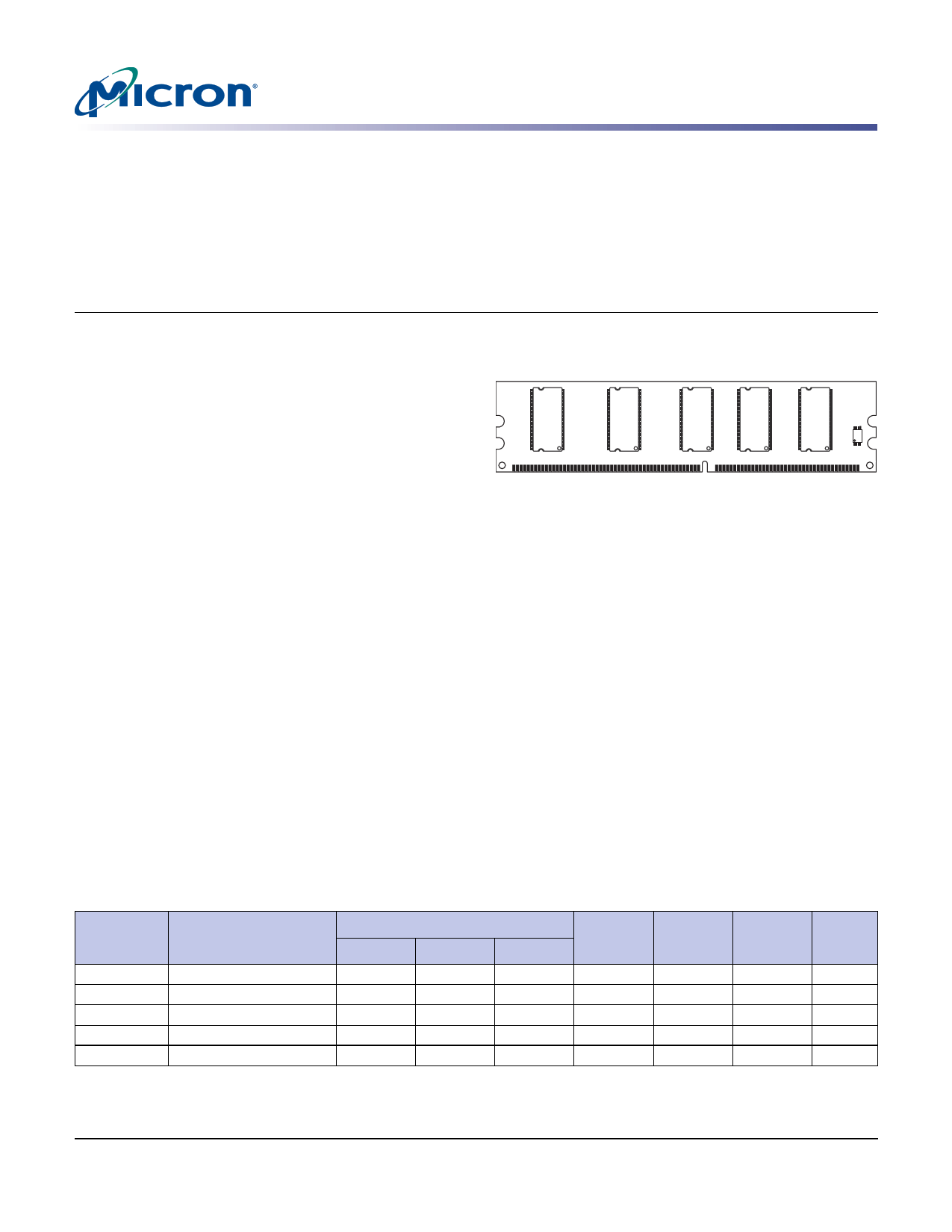
Figure 1: 184-Pin UDIMM (MO-206 R/C C)
PCB height: 31.75mm (1.25in)
Options
• Operating temperature3
– Commercial (0°C ≤ TA ≤ +70°C)
– Industrial (–40°C ≤ TA ≤ +85°C)
• Package
– 184-pin DIMM (standard)
– 184-pin DIMM (Pb-free)
• Memory clock, speed, CAS latency
– 5.0ns (200 MHz), 400 MT/s, CL = 3.0
– 6.0ns (167 MHz), 333 MT/s, CL = 2.5
– 7.5ns (133 MHz), 266 MT/s, CL = 2.0
– 7.5ns (133 MHz), 266 MT/s, CL = 2.0
– 7.5ns (133 MHz), 266 MT/s, CL = 2.5
Marking
None
I
G
Y
-40B
-335
-262
-26A
-265
Notes: 1. End of life.
2. Not recommended for new designs.
3. Contact Micron for industrial temperature
module offerings.
Table 1: Key Timing Parameters
Speed
Grade
-40B
-335
-262
-26A
-265
Industry
Nomenclature
Data Rate (MT/s)
CL = 3 CL = 2.5 CL = 2
tRCD
(ns)
tRP
(ns)
tRC
(ns)
Notes
PC3200
PC2700
PC2100
PC2100
PC2100
400 333 266
15
15
55
–
333 266
18
18
60 1
–
266 266
15
15
60
–
266 266
20
20
65
–
266 200
20
20
65
Notes: 1. The values of tRCD and tRP for -335 modules show 18ns to align with industry specifications;
actual DDR SDRAM device specifications are 15ns.
PDF: 09005aef808143d9/Source: 09005aef806e1c40
DD5C8_16_32x72A.fm - Rev. F 10/07 EN
1 Micron Technology, Inc., reserves the right to change products or specifications without notice.
©2002 Micron Technology, Inc. All rights reserved.
Products and specifications discussed herein are subject to change by Micron without notice.
1 page 
64MB, 128MB, 256MB (x72, ECC, SR) 184-Pin DDR SDRAM UDIMM
Functional Block Diagram
Functional Block Diagram
Figure 2: Functional Block Diagram
S0#
DQS0
DM0/DQS9
DQ0
DQ1
DQ2
DQ3
DQ4
DQ5
DQ6
DQ7
DQS1
DM1/DQS10
DQ8
DQ9
DQ10
DQ11
DQ12
DQ13
DQ14
DQ15
UDQS
UDM
DQ
DQ
DQ
DQ
DQ
DQ
DQ
DQ
LDQS
LDM
DQ
DQ
DQ
DQ
DQ
DQ
DQ
DQ
S0#
U1
DQS4
DM4/DQS13
DQ32
DQ33
DQ34
DQ35
DQ36
DQ37
DQ38
DQ39
DQS5
DM5/DQS14
DQ40
DQ41
DQ42
DQ43
DQ44
DQ45
DQ46
DQ47
DQS2
DM2/DQS11
DQ16
DQ17
DQ18
DQ19
DQ20
DQ21
DQ22
DQ23
DQS3
DM3/DQS12
DQ24
DQ25
DQ26
DQ27
DQ28
DQ29
DQ30
DQ31
UDQS
UDM
DQ
DQ
DQ
DQ
DQ
DQ
DQ
DQ
LDQS
LDM
DQ
DQ
DQ
DQ
DQ
DQ
DQ
DQ
S0#
U2
DQS6
DM6/DQS15
DQ48
DQ49
DQ50
DQ51
DQ52
DQ53
DQ54
DQ55
DQS7
DM7/DQS16
DQ56
DQ57
DQ58
DQ59
DQ60
DQ61
DQ62
DQ63
UDQS
UDM
DQ
DQ
DQ
DQ
DQ
DQ
DQ
DQ
LDQS
LDM
DQ
DQ
DQ
DQ
DQ
DQ
DQ
DQ
S0#
U4
UDQS
UDM
DQ
DQ
DQ
DQ
DQ
DQ
DQ
DQ
LDQS
LDM
DQ
DQ
DQ
DQ
DQ
DQ
DQ
DQ
S0#
U5
DQS8
DM8/DQS17
CB0
CB1
CB2
CB3
CB4
CB5
CB6
CB7
VSS
VDD
NC
NC
NC
NC
NC
NC
NC
NC
UDQS
UDM
DQ
DQ
DQ
DQ
DQ
DQ
DQ
DQ
LDQS
LDM
DQ
DQ
DQ
DQ
DQ
DQ
DQ
DQ
S0#
U3
BA0–BA1
A0–A11/A12
RAS#
CAS#
WE#
CKE0
CK0
CK0#
CK1
CK1#
CK2
CK2#
DDR SDRAM
A0–A11/A12 DDR SDRAM
DDR SDRAM
DDR SDRAM
DDR SDRAM
DDR SDRAM
DDR SDRAM U3
DDR SDRAM U1, U2
DDR SDRAM U4, U5
U6
SCL SPD EEPROM
WP A0 A1 A2
VSS SA0 SA1 SA2
SDA
VDDSPD
VDD/VDDQ
VREF
VSS
SPD EEPROM
DDR SDRAM
DDR SDRAM
DDR SDRAM
PDF: 09005aef808143d9/Source: 09005aef806e1c40
DD5C8_16_32x72A.fm - Rev. F 10/07 EN
5 Micron Technology, Inc., reserves the right to change products or specifications without notice.
©2002 Micron Technology, Inc. All rights reserved.
5 Page 
64MB, 128MB, 256MB (x72, ECC, SR) 184-Pin DDR SDRAM UDIMM
Serial Presence-Detect
Serial Presence-Detect
Table 13: Serial Presence-Detect EEPROM DC Operating Conditions
Parameter/Condition
Supply voltage
Input high voltage: Logic 1; All inputs
Input low voltage: Logic 0; All inputs
Output low voltage: IOUT = 3mA
Input leakage current: VIN = GND to VDD
Output leakage current: VOUT = GND to VDD
Standby current: SCL = SDA = VDD - 0.3V; All other inputs = VSS or VDD
Power supply current: SCL clock frequency = 100 kHz
Symbol
VDDSPD
VIH
VIL
VOL
ILI
ILO
ISB
ICC
Min
Max
2.3
VDDSPD × 0.7
–1.0
–
–
–
–
–
3.6
VDDSPD + 0.5
VDDSPD × 0.3
0.4
10
10
30
2.0
Units
V
V
V
V
µA
µA
µA
mA
Table 14: Serial Presence-Detect EEPROM AC Operating Conditions
Parameter/Condition
SCL LOW to SDA data-out valid
Time the bus must be free before a new transition can start
Data-out hold time
SDA and SCL fall time
Data-in hold time
Start condition hold time
Clock HIGH period
Noise suppression time constant at SCL, SDA inputs
Clock LOW period
SDA and SCL rise time
SCL clock frequency
Data-in setup time
Start condition setup time
Stop condition setup time
WRITE cycle time
Symbol
tAA
tBUF
tDH
tF
tHD:DAT
tHD:STA
tHIGH
tI
tLOW
tR
fSCL
tSU:DAT
tSU:STA
tSU:STO
tWRC
Min
0.2
1.3
200
–
0
0.6
0.6
–
1.3
–
–
100
0.6
0.6
–
Max
0.9
–
–
300
–
–
–
50
–
0.3
400
–
–
–
10
Units
µs
µs
ns
ns
µs
µs
µs
ns
µs
µs
kHz
ns
µs
µs
ms
Notes
1
2
2
3
4
Notes:
1. To avoid spurious start and stop conditions, a minimum delay is placed between SCL = 1 and
the falling or rising edge of SDA.
2. This parameter is sampled.
3. For a restart condition or following a WRITE cycle.
4. The SPD EEPROM WRITE cycle time (tWRC) is the time from a valid stop condition of a write
sequence to the end of the EEPROM internal ERASE/PROGRAM cycle. During the WRITE
cycle, the EEPROM bus interface circuit is disabled, SDA remains HIGH due to pull-up resis-
tance, and the EEPROM does not respond to its slave address.
Serial Presence-Detect Data
For the latest serial presence-detect data, refer to Micron’s SPD page:
www.micron.com/SPD.
PDF: 09005aef808143d9/Source: 09005aef806e1c40
DD5C8_16_32x72A.fm - Rev. F 10/07 EN
11
Micron Technology, Inc., reserves the right to change products or specifications without notice.
©2002 Micron Technology, Inc. All rights reserved.
11 Page | ||
| Páginas | Total 12 Páginas | |
| PDF Descargar | [ Datasheet MT5VDDT1672A.PDF ] | |
Hoja de datos destacado
| Número de pieza | Descripción | Fabricantes |
| MT5VDDT1672A | 128MB DDR SDRAM UDIMM | Micron |
| MT5VDDT1672H | 128MB DDR SDRAM Small-Outline DIMM | Micron |
| Número de pieza | Descripción | Fabricantes |
| SLA6805M | High Voltage 3 phase Motor Driver IC. |
Sanken |
| SDC1742 | 12- and 14-Bit Hybrid Synchro / Resolver-to-Digital Converters. |
Analog Devices |
|
DataSheet.es es una pagina web que funciona como un repositorio de manuales o hoja de datos de muchos de los productos más populares, |
| DataSheet.es | 2020 | Privacy Policy | Contacto | Buscar |