|
|
|
PDF MT36VDDF25672 Data sheet ( Hoja de datos )
| Número de pieza | MT36VDDF25672 | |
| Descripción | 2GB DDR SDRAM RDIMM | |
| Fabricantes | Micron | |
| Logotipo | ||
Hay una vista previa y un enlace de descarga de MT36VDDF25672 (archivo pdf) en la parte inferior de esta página. Total 20 Páginas | ||
|
No Preview Available !
1GB, 2GB (x72, ECC, DR) 184-Pin DDR SDRAM RDIMM
Features
DDR SDRAM RDIMM
MT36VDDF12872 – 1GB
MT36VDDF25672 – 2GB
For component data sheets, refer to Micron’s Web site: www.micron.com
Features
• 184-pin, registered dual in-line memory module
(RDIMM)
• Tall- and standard-height PCB options
• Fast data transfer rates: PC2100, PC2700, or PC3200
• 1GB (128 Meg x 72) and 2GB (256 Meg x 72)
• Supports ECC error detection and correction
• VDD = VDDQ = +2.5V
(-40B VDD = VDDQ = +2.6V)
• VDDSPD = +2.3V to +3.6V
• 2.5V I/O (SSTL_2-compatible)
• Internal, pipelined double data rate (DDR)
2n-prefetch architecture
• Bidirectional data strobe (DQS) transmitted/
received with data—that is, source-synchronous
data capture
• Differential clock inputs (CK and CK#)
• Multiple internal device banks for concurrent
operation
• Dual rank
• Selectable burst lengths (BL): 2, 4, or 8
• Auto precharge option
• Auto refresh and self refresh modes: 7.8125µs
maximum average periodic refresh interval
• Serial presence-detect (SPD) with EEPROM
• Selectable CAS latency (CL) for maximum
compatibility
• Gold edge contacts
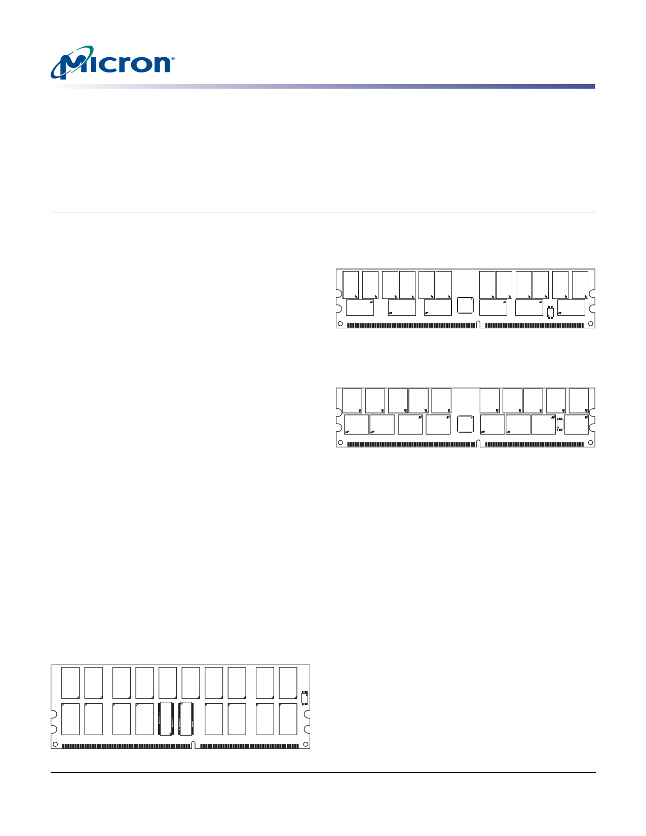
184-Pin RDIMM Figures
Figure 1: Tall-Height Layout – 1GB, 2GB
(MO-206-EA)
PCB height: 43.18mm (1.7in)
Figure 2: Standard-Height Layout – 1GB
(MO-206-CA R/C D)
PCB height: 30.48mm (1.2in)
Figure 3: Standard-Height Layout – 2GB
(MO-206-CA R/C D)
PCB height: 30.48mm (1.2in)
Options
• Operating temperature1
– Commercial (0°C ≤ TA ≤ +70°C)
– Industrial (–40°C ≤ TA ≤ +85°C)
• Package
– 184-pin DIMM (standard)
– 184-pin DIMM (Pb-free)
• Memory clock, speed, CAS latency2
– 5.0ns (200 MHz), 400 MT/s, CL = 3
– 6.0ns (166 MHz), 333 MT/s, CL = 2.5
– 7.5ns (133 MHz), 266 MT/s, CL = 2
– 7.5ns (133 MHz), 266 MT/s, CL = 2
– 7.5ns (133 MHz), 266 MT/s, CL = 2.5
Marking
None
I
G
Y
-40B
-335
-262
-26A
-265
Notes: 1. Contact Micron for industrial temperature
module offerings.
2. CL = CAS (READ) latency; registered mode
adds one clock cycle to CL.
PDF: 09005aef80772fd2/Source: 09005aef8075ebf6
DDF36C128_256x72.fm - Rev. G 9/08 EN
1 Micron Technology, Inc., reserves the right to change products or specifications without notice.
©2002 Micron Technology, Inc. All rights reserved.
Products and specifications discussed herein are subject to change by Micron without notice.
1 page 
1GB, 2GB (x72, ECC, DR) 184-Pin DDR SDRAM RDIMM
Pin Assignments and Descriptions
Table 6: Pin Descriptions
Symbol
A0–A12
BA0, BA1
CK0, CK0#
CKE0, CKE1
RAS#, CAS#, WE#
RESET#
S0#, S1#
SA0–SA2
SCL
CB0–CB7
DQ0–DQ63
DQS0–DQS17
SDA
VDD/VDDQ
VDDSPD
VREF
VSS
NC
Type
Input
Input
Input
Input
Input
Input
Input
Input
Input
I/O
I/O
I/O
I/O
Supply
Supply
Supply
Supply
–
Description
Address inputs: Provide the row address for ACTIVE commands, and the
column address and auto precharge bit (A10) for READ/WRITE commands, to
select one location out of the memory array in the respective device bank. A10
sampled during a PRECHARGE command determines whether the PRECHARGE
applies to one device bank (A10 LOW, device bank selected by BA0, BA1) or all
device banks (A10 HIGH). The address inputs also provide the op-code during a
MODE REGISTER SET command. BA0 and BA1 define which mode register
(mode register or extended mode register) is loaded during the LOAD MODE
REGISTER command.
Bank address: BA0 and BA1 define the device bank to which an ACTIVE,
READ, WRITE, or PRECHARGE command is being applied.
Clock: CK and CK# are differential clock inputs. All address and control input
signals are sampled on the crossing of the positive edge of CK and the
negative edge of CK#. Output data (DQ and DQS) is referenced to the
crossings of CK and CK#.
Clock enable: CKE enables (registered HIGH) and CKE disables (registered
LOW) the internal clock, input buffers, and output drivers.
Command inputs: RAS#, CAS#, and WE# (along with S#) define the command
being entered.
Reset: Asynchronously forces all registered outputs LOW when RESET# is LOW.
This signal can be used during power-up to ensure that CKE is LOW and DQ are
High-Z.
Chip selects: S# enables (registered LOW) and disables (registered HIGH) the
command decoder.
Presence-detect address inputs: These pins are used to configure the SPD
EEPROM address range on the I2C bus.
Serial clock for SPD EEPROM: SCL is used to synchronize the presence-detect
data transfer to and from the module.
Check bits.
Data input/output: Data bus.
Data strobe: Output with read data. Edge-aligned with read data. Input with
write data. Center-aligned with write data. Used to capture data.
Serial data: SDA is a bidirectional pin used to transfer addresses and data into
and out of the presence-detect portion of the module.
Power supply: +2.5V ±0.2V (-40B: +2.6V ±0.1V).
SPD EEPROM power supply: +2.3V to +3.6V.
SSTL_2 reference voltage (VDD/2).
Ground.
No connect: These pins are not connected on the module.
PDF: 09005aef80772fd2/Source: 09005aef8075ebf6
DDF36C128_256x72.fm - Rev. G 9/08 EN
5 Micron Technology, Inc., reserves the right to change products or specifications without notice.
©2002 Micron Technology, Inc. All rights reserved.
5 Page 
1GB, 2GB (x72, ECC, DR) 184-Pin DDR SDRAM RDIMM
Electrical Specifications
DRAM Operating Conditions
Recommended AC operating conditions are given in the DDR component data sheets.
Component specifications are available on Micron’s Web site. Module speed grades
correlate with component speed grades, as shown in table 8.
Table 8:
Module and Component Speed Grades
DDR components may exceed the listed module speed grades
Module Speed Grade
-40B
-335
-262
-26A
-265
Component Speed Grade
-5B
-6
-75E
-75Z
-75
Design Considerations
Simulations
Power
Micron memory modules are designed to optimize signal integrity through carefully
designed terminations, controlled board impedances, routing topologies, trace length
matching, and decoupling. However, good signal integrity starts at the system level.
Micron encourages designers to simulate the signal characteristics of the system’s
memory bus to ensure adequate signal integrity of the entire memory system.
Operating voltages are specified at the DRAM, not at the edge connector of the module.
Designers must account for any system voltage drops at anticipated power levels to
ensure the required supply voltage is maintained.
PDF: 09005aef80772fd2/Source: 09005aef8075ebf6
DDF36C128_256x72.fm - Rev. G 9/08 EN
11
Micron Technology, Inc., reserves the right to change products or specifications without notice.
©2002 Micron Technology, Inc. All rights reserved.
11 Page | ||
| Páginas | Total 20 Páginas | |
| PDF Descargar | [ Datasheet MT36VDDF25672.PDF ] | |
Hoja de datos destacado
| Número de pieza | Descripción | Fabricantes |
| MT36VDDF25672 | 2GB DDR SDRAM RDIMM | Micron |
| Número de pieza | Descripción | Fabricantes |
| SLA6805M | High Voltage 3 phase Motor Driver IC. |
Sanken |
| SDC1742 | 12- and 14-Bit Hybrid Synchro / Resolver-to-Digital Converters. |
Analog Devices |
|
DataSheet.es es una pagina web que funciona como un repositorio de manuales o hoja de datos de muchos de los productos más populares, |
| DataSheet.es | 2020 | Privacy Policy | Contacto | Buscar |