|
|
|
PDF WD3132 Data sheet ( Hoja de datos )
| Número de pieza | WD3132 | |
| Descripción | 38V Step-Up White LED Driver | |
| Fabricantes | WillSEMI | |
| Logotipo | ||
Hay una vista previa y un enlace de descarga de WD3132 (archivo pdf) en la parte inferior de esta página. Total 13 Páginas | ||
|
No Preview Available !
WD3132
High Efficiency, 38V Step-Up White LED
Driver for Medium LCD Panel Backlight
WD3132
Http//:www.sh-willsemi.com
Descriptions
The WD3132 is a constant current, high efficiency LED
driver. Internal MOSFET can drive up to 10 white LEDs
in series and 10S4P / 8S5P LEDs with 38V OVP. Peak
inductor current limit is larger than 1.5A. For LED
dimming, a Pulse-Width-Modulation (PWM) signal can
be applied to the EN pin. The device operates at
optimized 600k Hz fixed switching frequency to reduce
output ripple, improve conversion efficiency, and
allows use small external components.
The WD3132 is available in SOT-23-6L package.
Standard product is Pb-free and Halogen-free.
Features
Input voltage range
: 3~5.5V
Open LED Protection
: 38V
Reference Voltage
: 200mV (±5%)
Switching frequency
: 600k Hz (Typ.)
Efficiency
: Up to 92% (10S4P)
Main switch current limit : 1.5A (Min.)
PWM Dimming frequency : 5KHz to 200KHz
PWM Dimming Duty
: Min. 4%
Applications
Smart Phones
Tablets
Portable games
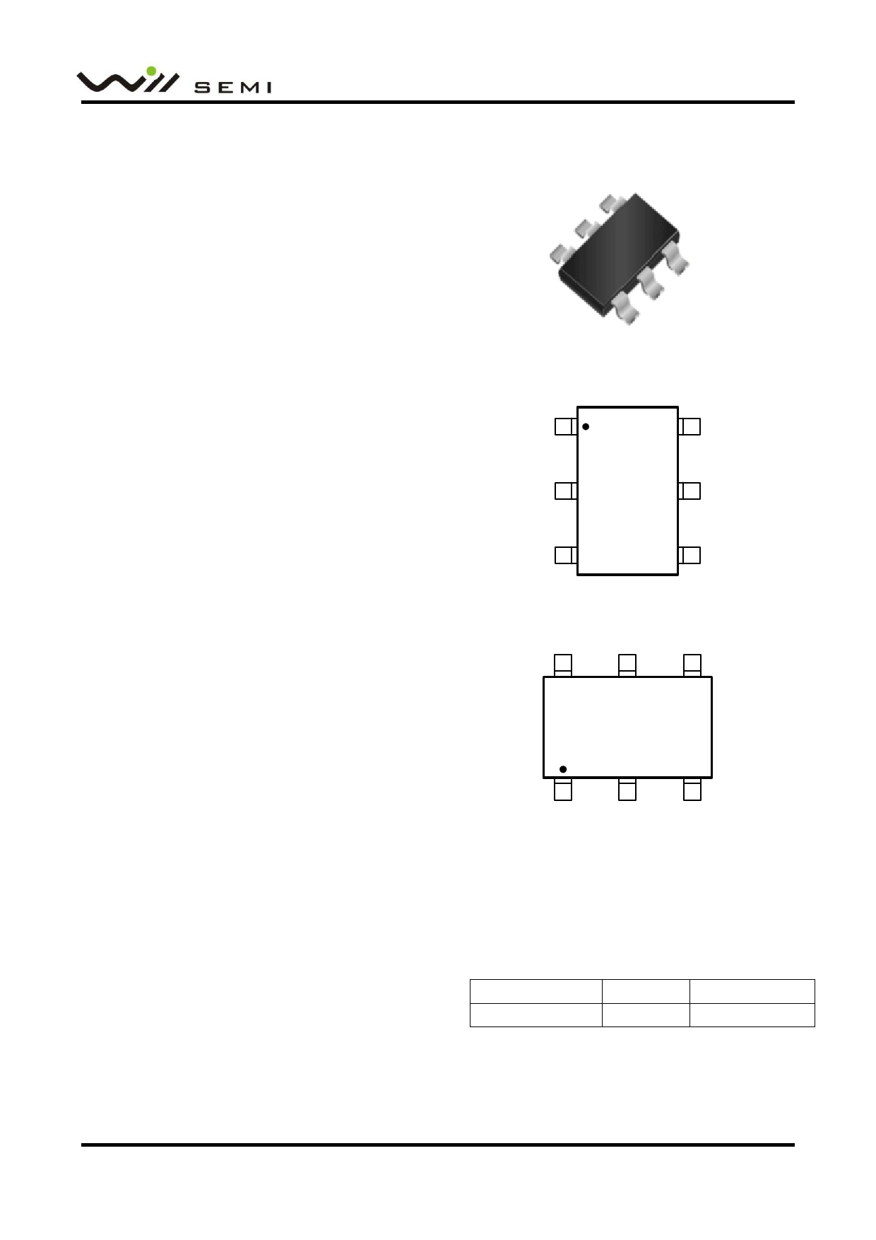
SOT-23-6L
LX 1
GND 2
6 VIN
5 OVP
FB 3
4 EN
Pin configuration (Top view)
654
3132
EAYW
123
3132 = Device Code
EA = Package Code
Y = Year code
W = Week code
Marking
Order information
Device
Package
Shipping
WD3132E-6/TR SOT-23-6L 3000/Reel&Tape
Will Semiconductor Ltd.
1 Jul, 2015 - Rev. 2.1
1 page 
Typical Characteristics (Ta=25oC, unless otherwise noted)
WD3132
95
90
85
80
75
70
L=10uH,10S4P LEDs
65 VIN = 3.2 V
VIN = 3.6 V
60 VIN = 4.2 V
VIN = 5 V
55
0 10 20 30 40 50 60 70 80
LED Current ( mA )
95
90
85
80
75
70
L=22uH,10S4P LEDs
65 VIN = 3.2 V
VIN = 3.6 V
60 VIN = 4.2 V
VIN = 5 V
55
0 10 20 30 40 50 60 70 80
LED Current ( mA )
Efficiency vs. Output Current
Efficiency vs. Output Current
95
90
85
80
75
70 L=10uH,8S5P LEDs
VIN = 3.2 V
65 VIN = 3.6 V
VIN = 4.2 V
60 VIN = 5 V
55
0 10 20 30 40 50 60 70 80 90 100
LED Current ( mA )
Efficiency vs. Output Current
95
90
85
80
75
70
L=22uH,8S5P LEDs
65 VIN = 3.2 V
VIN = 3.6 V
60 VIN = 4.2 V
VIN = 5 V
55
0 10 20 30 40 50 60 70 80 90 100
LED Current ( mA )
Efficiency vs. Output Current
84
82
80
78
76
3.0
L=10 uH
R =2.5
SET
3.5 4.0 4.5 5.0
Supply Voltage ( V )
5.5
LED Current vs. Supply Voltage
Will Semiconductor Ltd.
84
82
80
78
76
-40 -20
L=10uH
V =3.6V
IN
R =2.5
SET
0 20 40 60 80
Temperature(oC)
LED Current vs. Temperature
5 Jul, 2015 - Rev. 2.1
5 Page 
PCB Layout Considerations
A good circuit board layout aids in extracting the
most performance from the WD3132. Poor circuit
layout degrades the output ripple and the
electromagnetic interference (EMI) or electro-
magnetic compatibility (EMC) performance. The
evaluation board layout is optimized for the WD3132.
Use this layout for best performance. If this layout
needs changing, use the following guidelines:
1. Use separate analog and power ground planes.
Connect the sensitive analog circuitry (such as
voltage divider components) to analog ground;
connect the power components (such as input
and output bypass capacitors) to power ground.
Connect the two ground planes together near
the load to reduce the effects of voltage
dropped on circuit board traces. Locate CIN as
close to the VIN pin as possible, and use
separate input bypass capacitors for the
analog.
2. Route the high current path from CIN, through L
to the LX and GND pins as short as possible.
3. Keep high current traces as short and wide as
possible.
4. The output filter of the boost converter is also
critical for layout. The Diode and Output
capacitors should be placed to minimize the
area of current loop through Output –GND–LX.
5. Avoid routing high impedance traces, such as
Output, near the high current traces and
components or near the Diode node.
6. If high impedance traces are routed near high
current and/or the LX node, place a ground
plane shield between the traces.
7. Place the RSET resistor as close as possible to
FB pin, for the FB is a high impedance input pin
which is susceptible to noise.
WD3132
WD3132 PCB Suggest Layout (Demo)
Will Semiconductor Ltd.
11 Jul, 2015 - Rev. 2.1
11 Page | ||
| Páginas | Total 13 Páginas | |
| PDF Descargar | [ Datasheet WD3132.PDF ] | |
Hoja de datos destacado
| Número de pieza | Descripción | Fabricantes |
| WD3131 | 26V Step-Up White LED Driver | WillSEMI |
| WD3132 | 38V Step-Up White LED Driver | WillSEMI |
| WD3133 | 1.2-MHz DC-DC STEP-UP CONVERTERS | WillSEMI |
| WD3138 | White LED Driver | WillSEMI |
| Número de pieza | Descripción | Fabricantes |
| SLA6805M | High Voltage 3 phase Motor Driver IC. |
Sanken |
| SDC1742 | 12- and 14-Bit Hybrid Synchro / Resolver-to-Digital Converters. |
Analog Devices |
|
DataSheet.es es una pagina web que funciona como un repositorio de manuales o hoja de datos de muchos de los productos más populares, |
| DataSheet.es | 2020 | Privacy Policy | Contacto | Buscar |