|
|
|
PDF M5M4464P-15 Data sheet ( Hoja de datos )
| Número de pieza | M5M4464P-15 | |
| Descripción | 256K-Bit DRAM | |
| Fabricantes | Mitsubishi | |
| Logotipo | ||
Hay una vista previa y un enlace de descarga de M5M4464P-15 (archivo pdf) en la parte inferior de esta página. Total 15 Páginas | ||
|
No Preview Available !
MITSUBISHI LSls
MsM4464P-12, -15
262 144-BIT(65 536-WORD BY 4-BIT) DYNAMIC RAM
DESCRIPTION
This is family of 65536-word by 4-bit dynamic RAMs,
fabricated with the high performance N-channel silicon-gate
MOS process, and is ideal for large-ca-pacity memory
systems where high speed, low power dissipation, and low
costs are essential. The use of double-layer polysilicon
process technology and a single-transistor dynamic storage
cell provide high circuit density at reduced costs, and the
use of dynamic circuitry including sense amplifiers assures
low power dissipation. Multiplexed address inputs permit
both a reduction in pins to the standard l8-pin package
configuration and an increase in system densities. The
M5M4464P operates on a 5V power supply using the
on-chip substrate bias generator.
FEATURES
• Performance ranges
Type name
M5M4464P-12
M5M4464P-15
Access time
(max)
(ns)
120
150
Cycle time
(min)
Ins I
220
260
Power dissipation
"ypl
ImWI
260
230
• 65536 x 4 Organization
• Industry standard l8-pin dual in line package
• Single 5V±lO% supply
• Low standby power dissipation:
22mW (max)
• Low operating power dissipation:
M5M4464P-12
360mW (max)
M5M4464P-15
330mW (max)
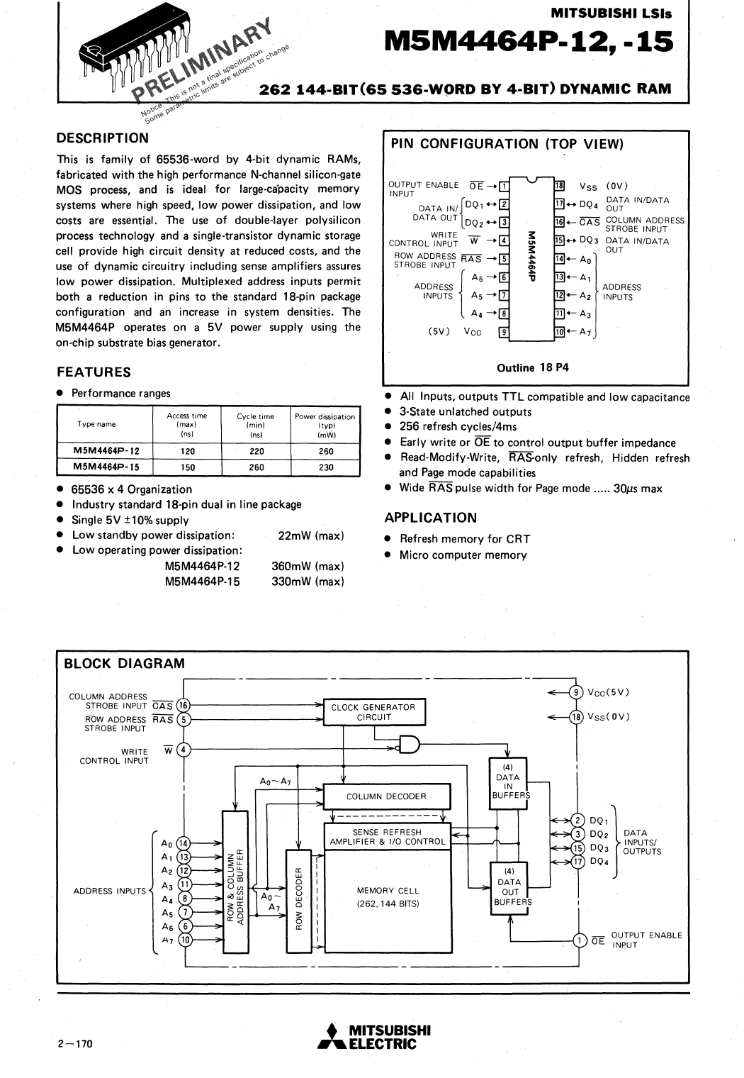
PIN CONFIGURATION (TOP VIEW)
OUTPUT ENABLE 0 E -+ 1
INPUT
DATA IN/{DQ' ... 2
DATA OUT DQ2'" 3
WRITE -
CONTROL INPUT W -+ 4
1~~ri6~~~~~i RAS -+ 5
ADIDNRPUESTSS
A5 -+ 7
A4 -+ 8
(5V) Vee
Vss (OV)
17 ... DQ4 g~iA IN/DATA
16 .... CAS COLUMN ADDRESS
STROBE. INPUT
15 ... DQ3 DATA IN/DATA
OUT
ADDRESS
INPUTS
Outline 18 P4
• All Inputs, outputs TTL compatible and low capacitance
• 3-State unlatched outputs
• 256 refresh cycles/4ms
• Early write or OE to control output buffer impedance
• Read-Modify-Write, RAS-only refresh, Hidden refresh
and Page mode capabilities
• Wide RAS pulse width for Page mode ..... 30tls max
APPLICATION
• Refresh memory for CRT
• Micro computer memory
BLOCK DIAGRAM
COLUSTMRNOBAEDDINREPSUST CAS 16'}----------~r;:~;:;_~:;_;;;;;:;;...,
ROW ADDRESS RAS 5 )---------.....,~.....,~~~~_...J
STROBE INPUT
WRITE
CONTROL INPUT
COLUMN DECODER
ADDRESS INPUTS
SENSE REFRESH
AMPLIFIER & I/O CONTROL
II:
Wuoo MEMORY CELL
ow (262. 144 BITSI
i3
II:
-19 Vee(5V)
18 Vss(OV)
DDQQ2 1} DATA
INPUTS/
DQ3 OUTPUTS
DQ4
OUTPUT ENABLE
INPUT
2-170
• .MITSUBISHI
.... ELECTRIC
1 page 
MITSUBISHI LSls
M5M4464P.12, ·15
262 144-BIT(6S S36·WORD BY 4-BIT) DYNAMIC RAM
SWITCHING CHARACTERISTICS (Ta=0-70'C, Vcc=5V±10%, Vss=ov, unless otherwise noted) INote 51
Symbol
Parall)eter
Alternative
Symbol
M5M4464P-12
Limits
Min Max
M5M4464P-15
limits
Min Max
Unit
ta(c)
Access time from CAS
INote 6,71 tCAC
60 75 ns
talA)
Access time from RAS
INote 6,81 t AAC
120 150 ns
ta (GE)
Access time from DE
INote 61
-
30 40 ns
tdiS(CH) Output disable time after CAS high
INote 91
tOFF
0 25 0 .30
tdiS(OE) Output disable time after DE high
INote 91
-
0 25 0 30
Note 5: An initial pause of 500#ls is required after power-up followed by any 8 -RA-S or -RAS/CAS cycles before proper device operation is achieved.
ns
ns
Note that RAS may be cycled during the initial pause.
And any 8 RAS or AAS/CAS cycles are required after prolonged periods (greater than 2msl of.RAS inactivity before proper device oper'ation is achieved.
6: Measured with a load circuit equivalent to 2TTL loads and 100pF.
7: Assume that tACCL ~ tALCL max.
<8: Assume that tALCL tALCL max. If tALCL is greater than tALCL max then ta(A) will increase by the amount that tRLCL exceeds tRLCL max.
9: t dis'(CH) max and tdis (DE) max define the time at which the output achieves the high impedance state (IOUT~ I ±1 oJ.l.AI ) and are not reference to VOH
min or VOL max.
TIMING REQUIREMENTS (For Read, Write, Read-Modify-Write, Refresh, and Page-Mode Cycles)
(Ta=0-70'C, Vcc=5V±10%, VSs=OV, unless otherwise noted, See notes 10,11)
Symbol
Parameter
Alternative
Symbol
M5M4464P-12
Limits
Min Max
M5M4464P-15
Limits
Min Max
Unit
tC(AF)
tW(RH)
Refresh cycle time
RAS high pulse width
t AEF
tAP
4 4 ms
90 100 ns
tALCL
tCHAL
tsu (AA)
tSU(CA)
th(AA)
th(CLCA)
th(ALCA)
tT
Delay time, RAS low to CAS low
Delay time, CAS high to RAS low
Row address setup time before RAS low
Column address setup time before CAS low
Row address hold time after RAS low
Column address hold time after CAS low
Column address hold time after RAS low
Transition time (rise and fall)
INote 121
(Note 131
INote 141
tACO
tCAP
tAS A
tASC
tAAH
tCAH
tAA
tT
25 60
10
0
0
15
20
80
3 50
30 75
10
0
0
20
25
100
3 50
ns
ns
ns
ns
ns
ns
ns
ns
Note 10:
11:
12:
13:
14:
The timing requirements are assumed tT=5ns
VIH min and VIL max are reference levels for measuring timing of input signals.
tRLCL max is specified as a reference point only; if tALCL is less than tRLcL max, access,time is ta(R), if tALCL is greater than tRLCL max, access time is
=tALCL + ta (C)· tALCL min is specified as tRLcL min. t h (RA) + 2 tT + tSU(CA).
tCHRL requirement is only applicable for RAS/CAS cycles preceeded by a CAS only cycle (i.e., For systems where CAS has not been decoded with RAS).
tT is measured between VIH min and VIL max.
Read and Refresh Cycles
Symbol
Parameter
Alternative
Symbol
to(rd)
tW(AL)
tW(CL)
tW(CH)
th (ALCH)
th (CLAH)
tsu (rd)
th(CHrd)
th (AHrd)
th (OECH)
th(OEAH)
th (CLOE)
th (ALOE)
t DOEL
tOEHD
t AHCL
Read cycle time
RAS low pulse width
CAS low pulse width
CAS high pulse width
CAS' hold time after RAS low
RAS hold time after CAS low
Read setup time before CAS low
Read hold time after CAS high
Read hold time after RAS high
CAS hold time after OE low
RAS hold time after OE low
OE hold time after CAS low
OE hold time after RAS low
Delay time, Data to OE low
Delay time,OE high to Data
Delay time, RAS high to CAS low
(Note 151
INote 151
t AC
t AAS
t CAS
tCPN
t CSH
tASH
t ACS
tACH
t ARH
-
-
-
-
-
-
-
Note 15: Either th(CHrd) or th(AHrd) must be satisfied for a read cycle,
M5M4464P-12
Limits
Min Max
220
120 10000
60
30
120
60
0
0
10
30
30
60
120
0
25
0
M5M4464P-15
Limits
Min Max
260
150 10000
75
35
150
75
0
0
10
40
40
75
150
0
30
0
Uf}it
ns
ns
ns
ns
ns
ns
ns
ns
ns
ns
ns
ns
ns
ns
ns
ns
2-174
• MITSUBISHI
.... ELECTRIC
5 Page 
MITSUBISHI LSls
M5M4464P-12, -IS
262 144-BIT(65 536-WORD BY 4-BIT) DYNAMIC RAM
Read-Write and Read-Modify-Write Cycles
RAS
th (RLCA)
to(rdW)
th(RLCH)
tWIRL)
th (CLRH)
tW(CL)
DQ,-DQ4
(INPUTS)
DQ,-DQ4
(OUTPUTS)
VOH -----~_H,gh-Z _...;.._ _ _-<1
VOL-
I. th (RLOE)
2-180
. • MITSUBISHI
"ELECTRIC
11 Page | ||
| Páginas | Total 15 Páginas | |
| PDF Descargar | [ Datasheet M5M4464P-15.PDF ] | |
Hoja de datos destacado
| Número de pieza | Descripción | Fabricantes |
| M5M4464P-12 | 256K-Bit DRAM | Mitsubishi |
| M5M4464P-15 | 256K-Bit DRAM | Mitsubishi |
| Número de pieza | Descripción | Fabricantes |
| SLA6805M | High Voltage 3 phase Motor Driver IC. |
Sanken |
| SDC1742 | 12- and 14-Bit Hybrid Synchro / Resolver-to-Digital Converters. |
Analog Devices |
|
DataSheet.es es una pagina web que funciona como un repositorio de manuales o hoja de datos de muchos de los productos más populares, |
| DataSheet.es | 2020 | Privacy Policy | Contacto | Buscar |