|
|
|
PDF M5M4257L-15 Data sheet ( Hoja de datos )
| Número de pieza | M5M4257L-15 | |
| Descripción | 256K-Bit DRAM | |
| Fabricantes | Mitsubishi | |
| Logotipo | ||
Hay una vista previa y un enlace de descarga de M5M4257L-15 (archivo pdf) en la parte inferior de esta página. Total 15 Páginas | ||
|
No Preview Available !
MITSUBISHI LSls
M5M4257L.12, ·15, ·20
262 144-BIT (262 144-WORD BY I-BIT) DYNAMIC RAM
DESCRIPTION
This is a family of 262 144-word by 1-bit dynamic RAMs,
fabricated with the high performance N-channel silicon gate
MOS process, and is ideal for large-capacity memory
systems where high speed, low power dissipation, and low
costs are essential. The use of double-layer polysilicon
process combined with silicide technology and a single-
transistor dynamic storage cell provide high circuit density
at reduced costs, and the use of dynamic circuitry including
sense amplifiers assures low power dissipation_ Multiplexed
address inputs permit both a reduction in pins to the 16 pin
zigzag inline package configuration and an increase in
system densities_ In addition to the RAS only refresh mode,
the Hidden refresh mode and CAS before RAS refresh
mode are available_
FEATURES
Type name
Access time
(max)
(ns)
Cycle tIme
(min)
(ns)
Power diSSipation
(typ)
(mW)
M5M4257L-12
120
230
260
M5M4257L-15
150
260
230
M5M4257L-20
200
330
190
• 16 pm zigzag mime package
• Single 5V±10% supply
• Low standby power dissipation:
25mW (max)
• Low operating power dissipation:
M5M4257L-12- - - - - ...... 360mW (max)
M5M4257L-15- .......... 330mW (max)
M5M4257 L-20 .... _ .. _... 275mW (max)
• Unlatched output enables two-dimensional chip selec-
tion
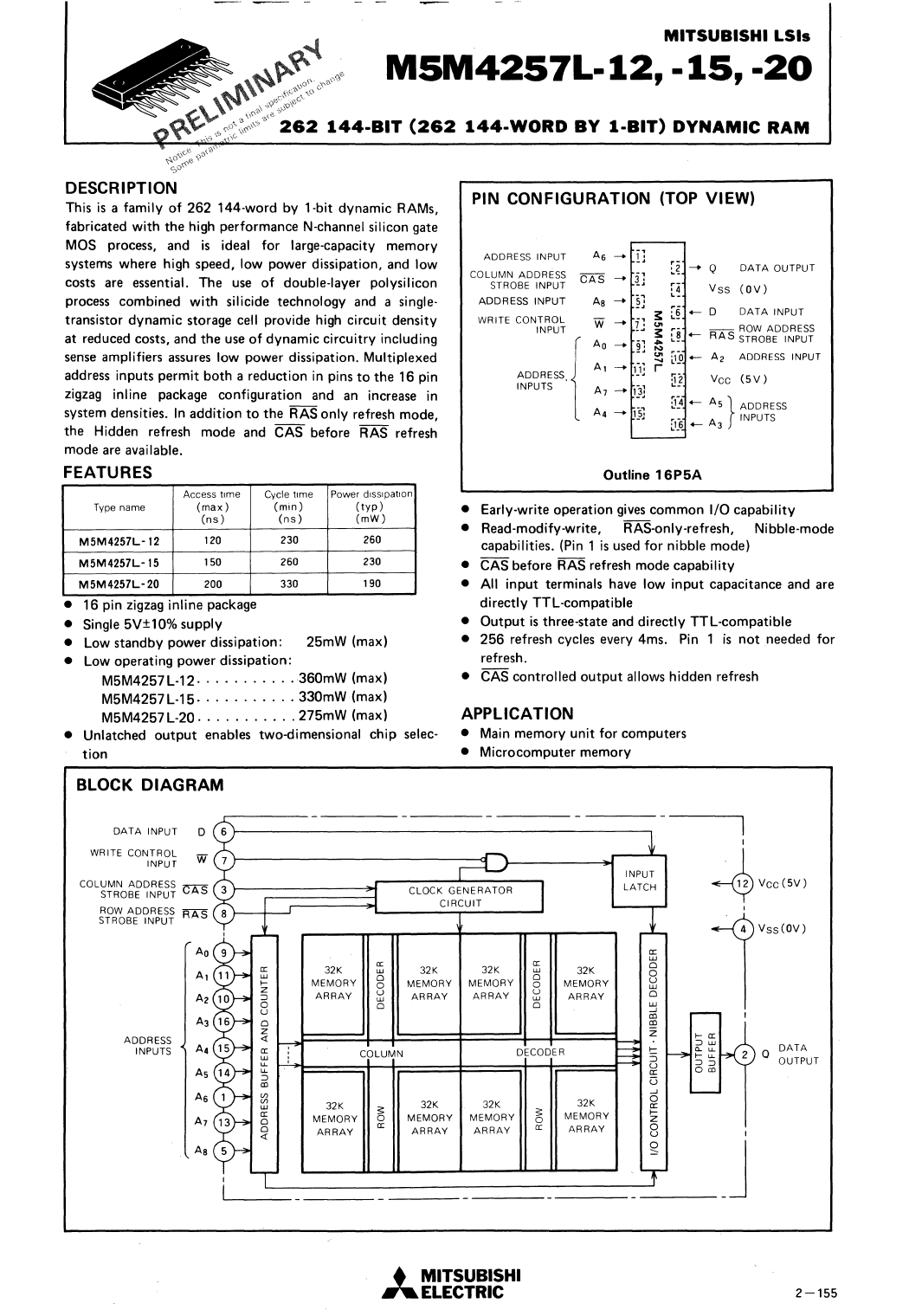
BLOCK DIAGRAM
PIN CONFIGURATION (TOP VIEW)
ADDRESS INPUT
As
i]
CDLUMN ADDRESS
STRDBE INPUT
CAS
i]
[~
[~
Q DATA DUTPUT
Vss (OV)
ADDRESS INPUT
WRITE CDNTRDL
INPUT
'"""" { .''r".".INPUTS
As
W
~J
fJ
~
~
[~
[~
+-D DATA INPUT
RAS ~~:D:~~~pE~i
Ao ~J
<.n i,-O +- A2 ADDRESS INPUT
A, -+ (lJ
L_
~j Vee (5V)
A7 -. 1)]
A4 -+ (5J
J:4 +- As } ADDRESS
[(6 +- A3 INPUTS
Outline 16P5A
• Early-write operation gives common I/O capability
• Read-modify-write, RAS-only-refresh, Nibble-mode
capabilities. (Pin 1 is used for nibble mode)
• CAS before RAS refresh mode capability
• All input terminals have low input capacitance and are
directly TTL-compatible
• Output is three-state and directly TTL-compatible
• 256 refresh cycles every 4ms. Pin 1 is not needed for
refresh.
• CAS controlled output allows hidden refresh
APPLICATION
• Main memory unit for computers
• Microcomputer memory
DATA INPUT
WRITE CDNTRDL
INPUT
D 6 ~------------------------------------------------,
W 7 ~----------------------------<I
INPUT
LATCH
ADDRESS
INPUTS
A,
A2
A3
A4
As
A7
32K
MEMDRY
ARRAY
a:
w
0
u0
w
0
32K
MEMDRY
ARRAY
32K
MEMDRY
ARRAY
cr:
w
0
0
::d
0
32K
MEMDRY
ARRAY
CDLUMN
DECDDER
32K
MEMDRY
ARRAY
~
0
a:
32K
MEMDRY
ARRAY
32K
MEMDRY
ARRAY
~
0
cr:
32K
MEMDRY
ARRAY
wcc
0
0uw
0
:':j
ccoo
Z
l-
Succ
U
..J
0
0:
Iz-
0u
~
I
~veC(5V)
,
1'%'"
DATA
DUTPUT
• MITSUBISHI
~ELECTRIC
2-155
1 page 
MITSUBISHI LSls
M5M4257L-12, -15, -20
262 i44-BIT (262 i44-WORD BY i-BIT) DYNAMIC RAM
TIMING REQUIREMENTS (For Read, Write, Read-Modify-Write, Refresh, and Nibble-Mode Cycle)
a -( Ta :: 70°C. Vee = 5V 1: 10%. v ss = OV. unless otherwise noted, See notes 5, 6 and 7 )
Symbol
Parameter
leAF
I W(RASH)
I W(RASL)
IW(CASL)
IW(CASH)
Ih (RAS-CAS)
Ih (CAS-RAS)
Id (CAS-RAS)
Id (RAS-CAS)
Isu (RA-RAS)
tSU(CA-CAS)
Ih (RAS-RA)
Ih (CAS-CA)
th (RAS-CA)
I THL
I TLH
Refresh cycle time
RAS high pulse width
RAS low pulse width
CAS low pulse width
rn high pulse width
CAS hold time after RAS
~ hold time after CAS
Delay time, CAS to RAS
Oelay time. RAS to CM
Row address setup time before RAS
Column address setup time before CAS
Rbw address hold lime after 'R'A'S
Column address hold time after CAS
Column address hold time. after AAS
Transition time
(Note 81
(Note 9)
(Note 10)
AI1ernative
Symbol
I REF
I'
RP
RAS
I CAS
ICPN
ICSH
IRSH
'CAP
IRCO
I ASR
IASC
I RAH
ICAH
I AR
IT
Limits
M5M4257L-12 M5M4257L-15 M5M4257L-20
Min Max Min Max Min Max
44
4
100 100 120
120 10000 150 10000 200 10000
60 75 100
30 35 40
120 150 200
60 75 100
30 30 40
25
60 25
75 30
100
000
0 -5 -5
15 20 25
20 25 35
80 100 135
3 50 3 50 3 50
Unit
ms
ns
ns
---
ns
ns
ns
ns
ns
ns
ns
ns
ns
ns
ns
ns
Note 5
6
9
10
An initial pause of 500~s is required after power-up followed by any eight RAS or RAS/CAS cycles before proper device operation IS achieved
= =The switching characteristics are defined as t THL t TLH 5ns.
Reference levels of input signals are VIH min. and V, L max, Reference levels for transition lime are also between VI Hand V IL .
Except for nibble-mode.
td (RAS-CAS) requirement is applicable for all AAS/CAS cycles
Operation within the td (RAS-CAS) max limit insures that ta (RAS)maX can be met. td (RAS-CAS)maX is specified reference point onlY,ii
td (RAS-CAS) is greater than the specified td (RAS-CAS) max limit. then access time is controlled exclusively by ta (CAS).
td (RAS-CAs)mm = t h (AAS-RA)mtn + 2t THL(t TU-,j + t SU(CA-CAS)mln.
SWITCHING CHARACTERISTICS (Ta=0-70'C, Vcc=5V±10%, VSs=OV, unlessotherwisenoted)
Read Cycle
Symbol
lOR
Isu (R-CAS)
Ih (CAS-R)
Ihl RAS-RI
tdls (CAS)
la(CAS)
la (RAS)
Parameter
Read cycle time
Read setup lime before CAS
Read hold time after CAS
Read hold time after RAS
Output disable time
CAS access time
RAS access time
(Note 1II
(Note 11)
(Note 12)
(Note 13)
(Note 14)
Alternative
Symbol
I RC
I RCS
I RCH
tRRH
IOFF
ICAC
I RAC
Limits
M5M4257L-12 M5M4257L-15 M5M4257L-20
Min Max Min Max Min Max
230 260 330
a0a
aaa
20 20 25
0 35
a 40
a 50
60 75 100
120 150 200
Unit
ns
ns
ns
ns
ns
ns
ns
Note 11
12
13
14
Either th (RAS-R) or th (CAS-A) must be satisfied for a read cycle.
tdls (CAS)maX defines the time at which the output achieves the open circuit conditllJn and is not reference to VOH or VOL
This is the value when td (RAS-CAS)~ td (RAS-CAS)ma)(, Test conditions. Load'" 2T TL. CL '" 100pF
This is the value when td (RAS-CAS)< t d (RAS-CAS)max. When td (RAS-CAS);;;: td (RAS-CAS)max. ta (RAS) Will Inuedse hy thp dllHllJ[lt lhilt
td (RAS- CAS) exceeds the value shown. Test conditions; Load = 2T TL C L '" 100pF
Write Cycle
Symbol
Parameter
low
Isu (W-CAS)
Ih (CAS-W)
Ih (RAS-W)
Ih (W-RAS)
Ih (W-CAS)
Iw(w)
Isu (D-CAS)
Ih (CAS-D)
Ih (RAS-O)
Write cycle time
Write setup time before CAS
Write hold time after CAS
Write hold ti me after RAS
RAS hold time after write
CAS hold time after write
Write pulse width
Data-in setup time before CAS
Data-in hold time after CAS
Data-in hold tillle after RAS
(Note 17)
Alternative
Symbol
I RC
IwCS
IWCH
I WCR
I RWL
ICWL
Iwp
loS
IOH
IOHR
Limits
M5M4257L- 12 M5M4257L-15 M5M4257L-20
Min Max Min Max Min Max
230 260 330
-5 -10 -10
40 45 55
100 120 155
40 45 55
40 45 55
40 45 55
a0a
30 35 40
90 110 140
Unit
ns
ns
ns
ns
ns
ns
ns
ns
ns
ns
• MITSUBISHI
..... ELECTRIC
2-159
5 Page 
MITSUBISHI LSls
M5M4257L-12, -15, -20
262 i44-BIT (262 i44-WORD BY i-BIT) DYNAMIC RAM
CAS before RAS Refresh Cycle (Note 221
REFRESH CYCLE
READ CYCLE
REFRESH CYCLE
teR
READ OR WRITE
CYCLE
VOH-
Q
}-------------------------~~-----HIGH IMPEDANCE S T A T E - - - - - - - - - - - - - - - - - - - - - -
VOL - _____- {
Note 22: W, 0 = don't care
TYPICAL CHARACTERISTICS
NORMALIZED ACCESS TIME
VS.SUPPLY VOLTAGE
1.3
;;;
::4:
1.2
."!
:g
1.1
l-
V>
~
uu 1.0
<l:
0
w
C:J
0.9
-"
:<:;l:;
a:
0z
0.8
, Ta~2S·C
I\.
\
I"" .........
"" ...........
0.7
4.0 S.O 6.0
NORMALIZED ACCESS TIME
VS. AMBIENT TEMPERATURE
1.3
"'::4:
1.2
."!
w
::;; 1.1
l-
V>
Vw>
uu 1.0
<l:
0
w
N
0.9
~
:<:;l;:
a: 0.8
0z
1 .1
Vee=S.OV
/
/
"
V
-,V
V
0.7-20
20 40 60 80 100
SUPPL Y VOLTAGE Vee (V)
AMBIENT TEMPERATURE Ta eC)
ACCESS TIME VS. LOAD
CAPACITANCE
S
1 .1
Vee=4.SV
'" 20 r- Ta =2S'C
.5
<fl
4:
II:
1S
<l 10
o
. /V
;'"
I
VV
V
-S 100 200 300 400 500 600
LOAD CAP'ACITANCE CL (pF)
NIBBLE MODE ACCESS TIME
VS. SUPPLY VOLTAGE
u; 1.6
<t
2-
Ta=2S~z
."! 1.4
U:;:J;
I\.
>= 1.2
(f)
(f)
UJ
«Uu 1.0
':J
''z"" 0.8
'"1"'-.......t--......
I'
0
UJ
«::N:;::;; 0.6
a:
0z 0.4
4.0
S.O
6.0
SUPPLY VOLTAGE Vee (V)
• MITSUBISHI
..... ELECTRIC
2-165
11 Page | ||
| Páginas | Total 15 Páginas | |
| PDF Descargar | [ Datasheet M5M4257L-15.PDF ] | |
Hoja de datos destacado
| Número de pieza | Descripción | Fabricantes |
| M5M4257L-12 | 256K-Bit DRAM | Mitsubishi |
| M5M4257L-15 | 256K-Bit DRAM | Mitsubishi |
| Número de pieza | Descripción | Fabricantes |
| SLA6805M | High Voltage 3 phase Motor Driver IC. |
Sanken |
| SDC1742 | 12- and 14-Bit Hybrid Synchro / Resolver-to-Digital Converters. |
Analog Devices |
|
DataSheet.es es una pagina web que funciona como un repositorio de manuales o hoja de datos de muchos de los productos más populares, |
| DataSheet.es | 2020 | Privacy Policy | Contacto | Buscar |